LT1054/LT1054L
APPLICATIONS INFORMATION
ground pin of the LT1054 must be less than the total of the
supply voltage minus the voltage loss due to the switches.
Thevoltagelossversusoutputcurrentduetotheswitches
canbefoundinTypicalPerformanceCharacteristics.Other
configurations such as the negative doubler can provide
higher output voltages at reduced output currents (see
Typical Applications).
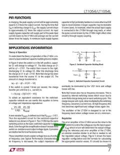
2.2µF
R3
V
IN
+
+
FB/SHDN
V
+
CAP
OSC
C
10µF
TANTALUM
+
IN
R4
LT1054
GND
R1
R2
V
REF
–
CAP
V
OUT
C1
RESTART SHUTDOWN
V
OUT
|V
REF
|
|V
|
OUT
R2
R1
OUT
=
+ 1 ≈
+ 1
Capacitor Selection
V
1.21V
C
OUT
– 40mV
)
)
)
)
100µF
TANTALUM
2
+
ForunregulatedcircuitsthenominalvaluesofC andC
WHERE V
= 2.5V NOMINAL
IN
OUT
REF
LT1054 • F05
should be equal. For regulated circuits see the section on
FOR EXAMPLE: TO GET V
PIN OF THE LT1054, CHOOSE R1 = 20k, THEN
= –5V REFERRED TO THE GROUND
OUT
Regulation. While the exact values of C and C
are
IN
OUT
|–5V|
noncritical, goodquality, lowESRcapacitorssuchassolid
R2 = 20k
+ 1 = 102.6k*
2.5V
)
)
– 40mV
tantalum are necessary to minimize voltage losses at high
currents. For C the effect of the ESR of the capacitor will
2
*CHOOSE THE CLOSEST 1% VALUE
IN
be multiplied by four due to the fact that switch currents
areapproximatelytwotimeshigherthanoutputcurrentand
losses will occur on both the charge and discharge cycle.
Figure 5
be 20k or greater because the reference output current
is limited to ≈100µA. R2 should be chosen to be in the
range of 100k to 300k. For optimum results the ratio of
This means that using a capacitor with 1Ω of ESR for C
IN
will have the same effect as increasing the output imped-
C /C
is recommended to be 1/10. C1, required for
IN OUT
ance of the LT1054 by 4Ω. This represents a significant
good load regulation at light load currents, should be
increaseinthevoltagelosses. ForC
theaffectofESRis
OUT
0.002µF for all output voltages.
less dramatic. C
is alternately charged and discharged
OUT
at a current approximately equal to the output current and
the ESR of the capacitor will cause a step function to oc-
cur in the output ripple at the switch transitions. This step
function will degrade the output regulation for changes
in output load current and should be avoided. Realizing
that large value tantalum capacitors can be expensive, a
technique that can be used is to parallela smaller tantalum
capacitor with a large aluminum electrolytic capacitor to
gain both low ESR and reasonable cost. Where physical
size is a concern some of the newer chip type surface
mount tantalum capacitors can be used. These capacitors
are normally rated at working voltages in the 10V to 20V
range and exhibit very low ESR (in the range of 0.1Ω).
A new die layout was required to fit into the physical
dimensions of the S8 package. Although the new die
of the LT1054CS8 will meet all the specifications of the
existing LT1054 data sheet, subtle differences in the
layout of the new die require consideration in some ap-
plication circuits. In regulating mode circuits using the
1054CS8 the nominal values of the capacitors, C and
IN
C
OUT
, must be approximately equal for proper operation
at elevated junction temperatures. This is different from
the earlier part. Mismatches within normal production
tolerances for the capacitors are acceptable. Making the
nominal capacitor values equal will ensure proper opera-
tion at elevated junction temperatures at the cost of a
small degradation in the transient response of regulator
Output Ripple
circuits. For unregulated circuits the values of C and
IN
C
OUT
are normally equal for all packages. For S8 applica-
The peak-to-peak output ripple is determined by the value
of the output capacitor and the output current. Peak-to-
peak output ripple may be approximated by the formula:
tions assistance in unusual applications circuits, please
consult the factory.
It can be seen from the circuit block diagram that the
maximumregulatedoutputvoltageislimitedbythesupply
voltage. For the basic configuration, |VOUT|referred to the
IOUT
dV =
2fCOUT
1054lfg
8

 Linear [ Linear ]