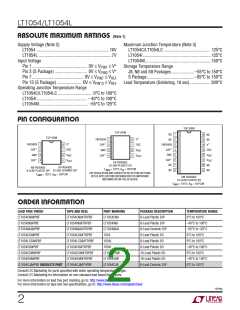
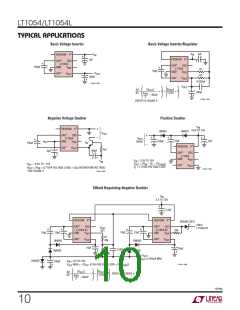
LT1054/LT1054L
PIN FUNCTIONS
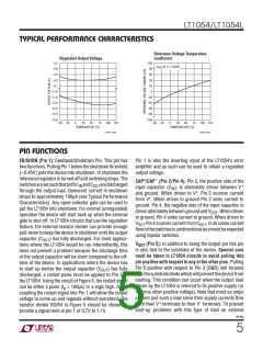
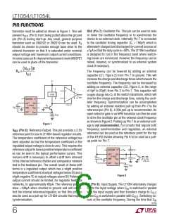
transistor must be added as shown in Figure 1. This will
OSC (Pin 7): Oscillator Pin. This pin can be used to raise
or lower the oscillator frequency or to synchronize the
device to an external clock. Internally Pin 7 is connected
prevent V
(Pin 5) from being pulled above the ground
OUT
pin (Pin 3) during start-up. Any small, general purpose
to the oscillator timing capacitor (C ≈ 150pF) which is
transistor such as 2N2222 or 2N2219 can be used. R
t
X
alternately charged and discharged by current sources of
7µAsothatthedutycycleis≈50ꢀ. TheLT1054oscillator
is designed to run in the frequency band where switch-
ing losses are minimized. However the frequency can be
raised, lowered, or synchronized to an external system
clock if necessary.
should be chosen to provide enough base drive to the
external transistor so that it is saturated under nominal
output voltage and maximum output current conditions.
In some cases an N-channel enhancement mode MOSFET
can be used in place of the transistor.
V
β
(
)
OUT
RX ≤
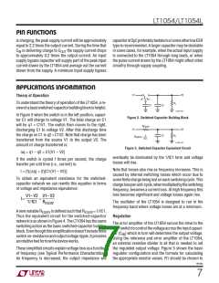
The frequency can be lowered by adding an external
capacitor (C1, Figure 2) from Pin 7 to ground. This will
increase the charge and discharge times which lowers the
oscillator frequency. The frequency can be increased by
adding an external capacitor (C2, Figure 2, in the range
of 5pF to 20pF) from Pin 2 to Pin 7. This capacitor will
IOUT
+
V
I
L
I
Q
+
–
LOAD
couple charge into C at the switch transitions, which will
T
I
OUT
+
shorten the charge and discharge time, raising the oscil-
lator frequency. Synchronization can be accomplished
by adding an external resistive pull-up from Pin 7 to the
reference pin (Pin 6). A 20k pull-up is recommended. An
open collector gate or an NPN transistor can then be used
to drive the oscillator pin at the external clock frequency
as shown in Figure 2. Pulling up Pin 7 to an external volt-
age is not recommended. For circuits that require both
frequency synchronization and regulation, an external
reference can be used as the reference point for the top
of the R1/R2 divider allowing Pin 6 to be used as a pull-
up point for Pin 7.
FB/SHDN
V
+
CAP
OSC
LT1054 • F01
+
R
LT1054
GND
X
C
IN
V
REF
–
CAP
V
OUT
C
OUT
+
Figure 1
V
(Pin 6): Reference Output. This pin provides a 2.5V
REF
referencepointforuseinLT1054-basedregulatorcircuits.
The temperature coefficient of the reference voltage has
been adjusted so that the temperature coefficient of the
regulated output voltage is close to zero. This requires the
referenceoutputtohaveapositivetemperaturecoefficient
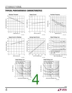
as can be seen in the typical performance curves. This
nonzero drift is necessary to offset a drift term inherent
in the internal reference divider and comparator network
tied to the feedback pin. The overall result of these drift
terms is a regulated output which has a slight positive
temperature coefficient at output voltages below 5V and a
slight negative TC at output voltages above 5V. Reference
output current should be limited, for regulator feedback
networks, to approximately 60µA. The reference pin will
draw ≈100µA when shorted to ground and will not af-
fect the internal reference/regulator, so that this pin can
also be used as a pull-up for LT1054 circuits that require
synchronization.
+
V
IN
FB/SHDN
V
C2
C1
+
CAP
OSC
+
LT1054
GND
C
IN
V
REF
LT1054 • F02
–
CAP
V
OUT
C
OUT
+
Figure 2
+
V (Pin 8): Input Supply. The LT1054 alternately charges
to the input voltage when C is switched in parallel
C
IN
IN
with the input supply and then transfers charge to C
OUT
when C is switched in parallel with C . Switching oc-
curs at the oscillator frequency. During the time that C
IN
OUT
IN
1054lfg
6

 Linear [ Linear ]