LTC3787
APPLICATIONS INFORMATION
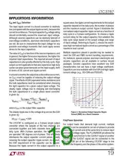
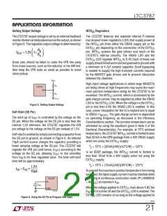
Setting Output Voltage
INTV Regulators
CC
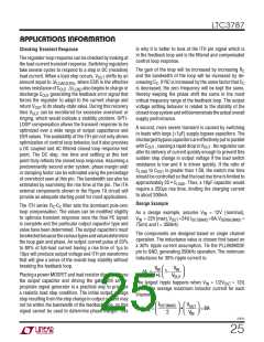
The LTC3787 output voltage is set by an external feedback
resistordividercarefullyplacedacrosstheoutput,asshown
in Figure 5. The regulated output voltage is determined by:
The LTC3787 features two separate internal P-channel
low dropout linear regulators (LDO) that supply power at
the INTV pin from either the VBIAS supply pin or the
CC
EXTV pin depending on the connection of the EXTV
CC
CC
⎛
⎞
RB
RA
pin. INTV powers the gate drivers and much of the
VOUT =1.2V 1+
CC
⎜
⎝
⎟
⎠
LTC3787’s internal circuitry. The VBIAS LDO and the
EXTV LDO regulate INTV to 5.4V. Each of these can
CC
CC
Great care should be taken to route the VFB line away
from noise sources, such as the inductor or the SW line.
Also keep the VFB node as small as possible to avoid
noise pickup.
supplyatleast50mAandmustbebypassedtogroundwith
a minimum of 4.7μF ceramic capacitor. Good bypassing
is needed to supply the high transient currents required
by the MOSFET gate drivers and to prevent interaction
between the channels.
V
OUT
High input voltage applications in which large MOSFETs
are being driven at high frequencies may cause the maxi-
mum junction temperature rating for the LTC3787 to be
R
B
LTC3787
VFB
R
A
exceeded. The INTV current, which is dominated by the
CC
3787 F05
gate charge current, may be supplied by either the VBIAS
LDO or the EXTV LDO. When the voltage on the EXTV
CC
CC
Figure 5. Setting Output Voltage
pin is less than 4.8V, the VBIAS LDO is enabled. In this
case, power dissipation for the IC is highest and is equal
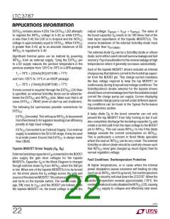
Soft-Start (SS Pin)
The start-up of V
to VBIAS • I
. The gate charge current is dependent
INTVCC
is controlled by the voltage on the
OUT
on operating frequency, as discussed in the Efficiency
Considerations section. The junction temperature can be
estimated by using the equations given in Note 3 of the
Electrical Characteristics. For example, at 70°C ambient
SS pin. When the voltage on the SS pin is less than the
internal 1.2V reference, the LTC3787 regulates the VFB
pin voltage to the voltage on the SS pin instead of 1.2V.
temperature, theLTC3787INTV currentislimitedtoless
CC
Soft-startisenabledbysimplyconnectingacapacitorfrom
the SS pin to ground, as shown in Figure 6. An internal
10μA current source charges the capacitor, providing a
linear ramping voltage at the SS pin. The LTC3787 will
than 32mA in the QFN package from a 40V VBIAS supply
when not using the EXTV supply:
CC
T = 70°C + (32mA)(40V)(43°C/W) = 125°C
J
regulate the VFB pin (and hence, V ) according to the
OUT
In an SSOP package, the INTV current is limited to
CC
voltage on the SS pin, allowing V
to rise smoothly
OUT
less than 15mA from a 40V supply when not using the
from V to its final regulated value. The total soft-start
IN
EXTV supply:
CC
time will be approximately:
T = 70°C + (15mA)(40V)(90°C/W) = 125°C
J
1.2V
10µA
tSS =CSS
•
To prevent the maximum junction temperature from being
exceeded, the input supply current must be checked while
operating in continuous conduction mode (PLLIN/MODE
LTC3787
SS
= INTV ) at maximum V .
CC
IN
C
SS
When the voltage applied to EXTV rises above 4.8V, the
SGND
CC
3787 F06
V LDO is turned off and the EXTV LDO is enabled. The
IN
CC
EXTV LDO remains on as long as the voltage applied to
CC
Figure 6. Using the SS Pin to Program Soft-Start
3787fc
21

 Linear Systems [ Linear Systems ]