LTC3787
APPLICATIONS INFORMATION
the entire LTC3787 chip. Once the junction temperature
input. When the external clock frequency is less than f
,
OSC
dropsbacktoapproximately155°C, theINTV LDOturns
current is sunk continuously, pulling down the VCO input.
If the external and internal frequencies are the same but
exhibit a phase difference, the current sources turn on for
an amount of time corresponding to the phase difference.
The voltage at the VCO input is adjusted until the phase
and frequency of the internal and external oscillators are
identical. At the stable operating point, the phase detector
output is high impedance and the internal filter capacitor,
CC
back on. Long term overstress (T > 125°C) should be
J
avoided as it can degrade the performance or shorten
the life of the part.
Since the shutdown may occur at full load, beware that
the load current will result in high power dissipation in
the body diodes of the top MOSFETs. In this case, PGOOD
output may be used to turn the system load off.
C
, holds the voltage at the VCO input.
LP
Phase-Locked Loop and Frequency Synchronization
Typically,theexternalclock(onthePLLIN/MODEpin)input
highthresholdis1.6V,whiletheinputlowthresholdis1.2V.
The LTC3787 has an internal phase-locked loop (PLL)
comprised of a phase frequency detector, a lowpass filter
and a voltage-controlled oscillator (VCO). This allows the
turn-on of the bottom MOSFET of channel 1 to be locked
to the rising edge of an external clock signal applied to
the PLLIN/MODE pin. The turn-on of channel 2’s bot-
tom MOSFET is thus 180 degrees out-of-phase with the
external clock. The phase detector is an edge-sensitive
digitaltypethatprovideszerodegreesphaseshiftbetween
the external and internal oscillators. This type of phase
detector does not exhibit false lock to harmonics of the
external clock.
Note that the LTC3787 can only be synchronized to an
external clock whose frequency is within range of the
LTC3787’s internal VCO, which is nominally 55kHz to
1MHz.Thisisguaranteedtobebetween75kHzand850kHz.
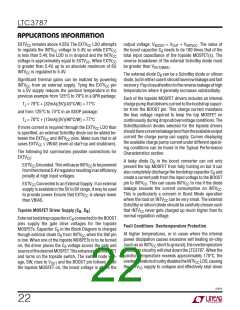
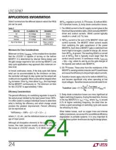
RapidphaselockingcanbeachievedbyusingtheFREQpin
to set a free-running frequency near the desired synchro-
nization frequency. The VCO’s input voltage is prebiased
at a frequency corresponding to the frequency set by the
FREQ pin. Once prebiased, the PLL only needs to adjust
the frequency slightly to achieve phase lock and synchro-
nization. Although it is not required that the free-running
frequency be near external clock frequency, doing so will
prevent the operating frequency from passing through a
large range of frequencies as the PLL locks.
If the external clock frequency is greater than the internal
oscillator’sfrequency,f ,thencurrentissourcedcontinu-
OSC
ously from the phase detector output, pulling up the VCO
1000
900
800
700
600
500
400
300
200
100
0
15 25 35 45 55 65 75 85 95 105 115 125
FREQ PIN RESISTOR (k)
3787 F07
Figure 7. Relationship Between Oscillator
Frequency and Resistor Value at the FREQ Pin
3787fc
23

 Linear Systems [ Linear Systems ]