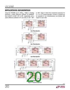
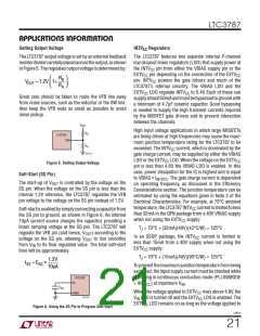
LTC3787
APPLICATIONS INFORMATION
Table 2 summarizes the different states in which the FREQ
pin can be used.
2
INTV regulator current, 3) I R losses, 4) bottom MOS-
CC
FET transition losses, 5) body diode conduction losses.
1. The VBIAS current is the DC supply current given in the
ElectricalCharacteristicstable,whichexcludesMOSFET
driver and control currents. VBIAS current typically
results in a small (<0.1%) loss.
Table 2.
FREQ PIN
PLLIN/MODE PIN
DC Voltage
FREQUENCY
350kHz
0V
INTV
DC Voltage
535kHz
CC
Resistor
DC Voltage
50kHz to 900kHz
2. INTV current is the sum of the MOSFET driver and
CC
Any of the Above
External Clock
Phase Locked to
External Clock
control currents. The MOSFET driver current results
from switching the gate capacitance of the power
MOSFETs. Each time a MOSFET gate is switched from
low to high to low again, a packet of charge, dQ, moves
Minimum On-Time Considerations
Minimum on-time, t , is the smallest time duration
that the LTC3787 is capable of turning on the bottom
MOSFET. It is determined by internal timing delays and
the gate charge required to turn on the top MOSFET. Low
duty cycle applications may approach this minimum on-
time limit.
from INTV to ground. The resulting dQ/dt is a current
CC
ON(MIN)
out of INTV that is typically much larger than the
CC
control circuit current. In continuous mode, I
GATECHG
= f(Q + Q ), where Q and Q are the gate charges of
T
B
T
B
the topside and bottom side MOSFETs.
2
3. DC I R losses. These arise from the resistances of the
MOSFETs,sensingresistor,inductorandPCboardtraces
andcausetheefficiencytodropathighoutputcurrents.
In forced continuous mode, if the duty cycle falls below
what can be accommodated by the minimum on-time,
the controller will begin to skip cycles but the output will
continuetoberegulated.Morecycleswillbeskippedwhen
4. Transition losses apply only to the bottom MOSFET(s),
and become significant only when operating at low
inputvoltages.Transitionlossescanbeestimatedfrom:
V increases. Once V rises above V , the loop keeps
IN
IN
OUT
the top MOSFET continuously on. The minimum on-time
for the LTC3787 is approximately 110ns.
3
I
VOUT
Transition Loss =(1.7)
•
OUT(MAX) •CRSS •f
2
V
IN
Efficiency Considerations
5. Body diode conduction losses are more significant at
higherswitchingfrequency. Duringthedeadtime, theloss
The percent efficiency of a switching regulator is equal to
the output power divided by the input power times 100%.
It is often useful to analyze individual losses to determine
what is limiting the efficiency and which change would
produce the greatest improvement. Percent efficiency
can be expressed as:
in the top MOSFETs is I
• V , where V is around
OUT
DS DS
0.7V. At higher switching frequency, the dead time be-
comes a good percentage of switching cycle and causes
the efficiency to drop.
Other hidden losses, such as copper trace and internal
batteryresistances,canaccountforanadditionalefficiency
degradation in portable systems. It is very important to
includethesesystem-levellossesduringthedesignphase.
%Efficiency = 100% – (L1 + L2 + L3 + ...)
where L1, L2, etc., are the individual losses as a percent-
age of input power.
Although all dissipative elements in the circuit produce
losses, five main sources usually account for most of
the losses in LTC3787 circuits: 1) IC VBIAS current, 2)
3787fc
24

 Linear Systems [ Linear Systems ]