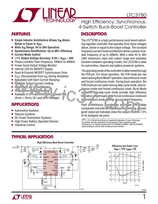
LTC3780
APPLICATIONS INFORMATION
The Standby Mode (STBYMD) Pin Function
Fault Conditions: Overvoltage Protection
Thestandbymode(STBYMD)pinprovidesseveralchoices
for start-up and standby operational modes. If the pin is
pulled to ground, the SS pin is internally pulled to ground,
preventing start-up and thereby providing a single control
pin for turning off the controller. If the pin is left open or
bypassedtogroundwithacapacitor,theSSpinisinternally
providedwithastartingcurrent,permittingexternalcontrol
for turning on the controller. If the pin is connected to a
A comparator monitors the output for overvoltage con-
ditions. The comparator (OV) detects overvoltage faults
greater than 7.5% above the nominal output voltage.
When the condition is sensed, switches A and C are
turned off, and switches B and D are turned on until the
overvoltage condition is cleared. During an overvoltage
condition, a negative current limit (V
= –60mV) is
SENSE
set to limit negative inductor current. When the sensed
currentinductorcurrentislowerthan–60mV,switchAand
C are turned on, and switch B and D are turned off until
the sensed current is higher than –20mV. If the output is
still in overvoltage condition, switch A and C are turned
off, and switch B and D are turned on again.
voltage greater than 1.25V, the internal regulator (INTV )
CC
will be on even when the controller is shut down (RUN
pin voltage < 1.5V). In this mode, the onboard 6V linear
regulator can provide power to keep-alive functions such
as a keyboard controller.
Fault Conditions: Current Limit and Current Foldback
Efficiency Considerations
The maximum inductor current is inherently limited in a
current mode controller by the maximum sense voltage.
In boost mode, maximum sense voltage and the sense
resistance determines the maximum allowed inductor
peak current, which is:
The percent efficiency of a switching regulator is equal to
the output power divided by the input power times 100%.
It is often useful to analyze individual losses to determine
what is limiting the efficiency and which change would
produce the most improvement. Although all dissipative
elements in circuit produce losses, four main sources
account for most of the losses in LTC3780 circuits:
160mV
IL(MAX,BOOST)
=
RSENSE
2
1. DC I R losses. These arise from the resistances of the
MOSFETs, sensing resistor, inductor and PC board
traces and cause the efficiency to drop at high output
currents.
In buck mode, maximum sense voltage and the sense
resistance determines the maximum allowed inductor
valley current, which is:
130mV
RSENSE
2. Transition loss. This loss arises from the brief amount
of time switch A or switch C spends in the saturated
region during switch node transitions. It depends upon
the input voltage, load current, driver strength and
MOSFET capacitance, among other factors. The loss
is significant at input voltages above 20V and can be
estimated from:
IL(MAX,BUCK)
=
To further limit current in the event of a short circuit to
ground, the LTC3780 includes foldback current limiting.
If the output falls by more than 30%, then the maximum
sense voltage is progressively lowered to about one third
of its full value.
–1
Transition Loss ≈ 1.7A • V • I
• C
• f
IN2 OUT
RSS
where C
is the reverse transfer capacitance.
RSS
3780fe
21

 Linear Systems [ Linear Systems ]