LTC3780
APPLICATIONS INFORMATION
• Use immediate vias to connect the components (in-
cluding the LTC3780’s SGND and PGND pins) to the
ground plane. Use several large vias for each power
component.
• Connect the top driver boost capacitor C closely to the
A
BOOST1 and SW1 pins. Connect the top driver boost
capacitor C closely to the BOOST2 and SW2 pins.
B
• Connect the input capacitors C and output capacitors
IN
• Use planes for V and V
to maintain good voltage
C
OUT
closely to the power MOSFETs. These capaci-
IN
OUT
filtering and to keep power losses low.
tors carry the MOSFET AC current in boost and buck
mode.
• Floodallunusedareasonalllayerswithcopper.Flooding
with copper will reduce the temperature rise of power
components. Connect the copper areas to any DC net
• Connect V
pin resistive dividers to the (+) termi-
OSENSE
nalsofC
andsignalground. AsmallV
bypass
OUT
OSENSE
(V or GND).
capacitormaybeconnectedcloselytotheLTC3780SGND
pin. The R2 connection should not be along the high
current or noise paths, such as the input capacitors.
IN
• Segregate the signal and power grounds. All small-
signal components should return to the SGND pin at
one point, which is then tied to the PGND pin close to
the sources of switch B and switch C.
–
+
• RouteSENSE andSENSE leadstogetherwithminimum
PC trace spacing. Avoid sense lines pass through noisy
area,suchasswitchnodes.Thefiltercapacitorbetween
• Place switch B and switch C as close to the controller
as possible, keeping the PGND, BG and SW traces
short.
+
–
SENSE and SENSE should be as close as possible
to the IC. Ensure accurate current sensing with Kelvin
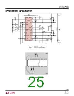
connections at the SENSE resistor. One layout example
is shown in Figure 12.
• Keep the high dV/dT SW1, SW2, BOOST1, BOOST2,
TG1 and TG2 nodes away from sensitive small-signal
nodes.
• Connect the I pin compensation network close to the
TH
IC, between I and the signal ground pins. The capaci-
TH
• The path formed by switch A, switch B, D1 and the C
tor helps to filter the effects of PCB noise and output
IN
capacitor should have shortleads andPCtracelengths.
voltage ripple voltage from the compensation loop.
The path formed by switch C, switch D, D2 and the
• ConnecttheINTV bypasscapacitor, C , closetothe
CC
VCC
C
capacitor also should have short leads and PC
OUT
trace lengths.
IC,betweentheINTV andthepowergroundpins.This
CC
capacitor carries the MOSFET drivers’ current peaks.
• Theoutputcapacitor(–)terminalsshouldbeconnected
as close as possible the (–) terminals of the input
capacitor.
Anadditional1μFceramiccapacitorplacedimmediately
next to the INTV and PGND pins can help improve
CC
noise performance substantially.
3780fe
24

 Linear Systems [ Linear Systems ]