LTC3780
APPLICATIONS INFORMATION
Double-check the T in the MOSFET with 70°C ambient
C is chosen to filter the square current in buck mode. In
J
IN
temperature:
this mode, the maximum input current peak is:
29%
2
⎛
⎝
⎞
T = 70°C + 1.94W • 40°C/W = 147.6°C
J
IIN,PEAK(MAX,BUCK) = 5s 1+
= 5.7A
⎜
⎟
⎠
The maximum power dissipation of switch B occurs in
buckmode. AssumingajunctiontemperatureofT =80°C
J
A low ESR (10mΩ) capacitor is selected. Input voltage
ripple is 57mV (assuming ESR dominate ripple).
with ρ
= 1.2, the power dissipation at V = 18V is:
80°C
IN
18–12
•52 •1.2•0.009 = 90mW
C
is chosen to filter the square current in boost mode.
OUT
PB,BUCK
=
18
In this mode, the maximum output current peak is:
12
5
11%
2
⎛
⎝
⎞
Double-check the T in the MOSFET at 70°C ambient
J
IOUT,PEAK(MAX,BOOST)
=
s5s 1+
=10.6A
⎜
⎟
⎠
temperature:
T = 70°C + 0.09W • 40°C/W = 73.6°C
J
A low ESR (5mΩ) capacitor is suggested. This capacitor
will limit output voltage ripple to 53mV (assuming ESR
dominate ripple).
ThemaximumpowerdissipationofswitchCoccursinboost
mode.AssumingajunctiontemperatureofT =110°Cwith
J
ρ
= 1.4, the power dissipation at V = 5V is:
110°C
IN
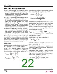
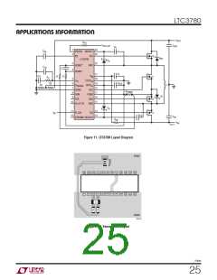
PC Board Layout Checklist
12–5 •12
(
)
PC,BOOST
=
•52 •1.4•0.009
The basic PC board layout requires a dedicated ground
plane layer. Also, for high current, a multilayer board
provides heat sinking for power components.
52
5
+ 2•123 • •150p•400k =1.27W
5
• The ground plane layer should not have any traces and
it should be as close as possible to the layer with power
MOSFETs.
Double-check the T in the MOSFET at 70°C ambient
J
temperature:
T = 70°C + 1.08W • 40°C/W = 113°C
J
•
Place C , switch A, switch B and D1 in one com-
IN
pact area. Place C , switch C, switch D and D2 in
The maximum power dissipation of switch D occurs
in boost mode when its duty cycle is higher than 50%.
OUT
one compact area. One layout example is shown in
Figure 10.
Assuming a junction temperature of T = 100°C with
J
ρ
= 1.35, the power dissipation at V = 5V is:
100°C
IN
V
SW2
SW1
V
OUT
IN
2
5
12
12
5
⎛
⎞
⎠
L
D2
QD
PD,BOOST
=
s
s5 s1ꢀ35s0ꢀ009= 0ꢀ73W
⎜
⎝
⎟
QA
Double-check the T in the MOSFET at 70°C ambient
J
D1
temperature:
QB
QC
T = 70°C + 0.73W • 40°C/W = 99°C
J
C
C
OUT
IN
R
SENSE
LTC3780
CKT
GND
3780 F10
Figure 10. Switches Layout
3780fe
23

 Linear Systems [ Linear Systems ]