LTC3780
APPLICATIONS INFORMATION
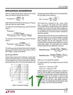
Schottky Diode (D1, D2) Selection
and Light Load Operation
INTV Regulator
CC
An internal P-channel low dropout regulator produces 6V
at the INTV pin from the V supply pin. INTV powers
TheSchottkydiodesD1andD2showninFigure1conduct
during the dead time between the conduction of the power
MOSFET switches. They are intended to prevent the body
diode of synchronous switches B and D from turning on
and storing charge during the dead time. In particular, D2
significantly reduces reverse recovery current between
switch D turn-off and switch C turn-on, which improves
converter efficiency and reduces switch C voltage stress.
In order for the diode to be effective, the inductance
between it and the synchronous switch must be as small
as possible, mandating that these components be placed
adjacently.
CC
IN
CC
the drivers and internal circuitry within the LTC3780. The
INTV pin regulator can supply a peak current of 40mA
CC
and must be bypassed to ground with a minimum of 4.7μF
tantalum,10μFspecialpolymerorlowESRtypeelectrolytic
capacitor. A1μFceramiccapacitorplaceddirectlyadjacent
to the INTV and PGND IC pins is highly recommended.
CC
Good bypassing is necessary to supply the high transient
current required by MOSFET gate drivers.
Higher input voltage applications in which large MOSFETs
are being driven at high frequencies may cause the maxi-
mum junction temperature rating for the LTC3780 to be
exceeded.Thesystemsupplycurrentisnormallydominated
by the gate charge current. Additional external loading of
In buck mode, when the FCB pin voltage is 0.85 < V
FCB
< 5V, the converter operates in skip-cycle mode. In this
mode, synchronous switch B remains off until the induc-
tor peak current exceeds one-fifth of its maximum peak
current. As a result, D1 should be rated for about one-half
to one-third of the full load current.
the INTV also needs to be taken into account for the
CC
power dissipation calculations. The total INTV current
CC
can be supplied by either the 6V internal linear regulator
or by the EXTV input pin. When the voltage applied to
CC
the EXTV pin is less than 5.7V, all of the INTV current
CC
CC
In boost mode, when the FCB pin voltage is higher than
5.3V,theconverteroperatesindiscontinuouscurrentmode.
In this mode, synchronous switch D remains off until the
inductor peak current exceeds one-fifth of its maximum
peak current. As a result, D2 should be rated for about
one-third to one-fourth of the full load current.
is supplied by the internal 6V linear regulator. Power dis-
sipation for the IC in this case is V • I , and overall
IN INTVCC
efficiency is lowered. The junction temperature can be
estimated by using the equations given in Note 2 of the
ElectricalCharacteristics.Forexample,atypicalapplication
operating in continuous current mode might draw 24mA
Inbuckmode,whentheFCBpinvoltageishigherthan5.3V,
the converter operates in constant frequency discontinu-
ous current mode. In this mode, synchronous switch B
remains on until the inductor valley current is lower than
the sense voltage representing the minimum negative
from a 24V supply when not using the EXTV pin:
CC
T = 70°C + 24mA • 24V • 34°C/W = 90°C
J
Use of the EXTV input pin reduces the junction tem-
CC
perature to:
inductor current level (V
= –5mV). Both switch A
SENSE
T = 70°C + 24mA • 6V • 34°C/W = 75°C
J
and B are off until next clock signal.
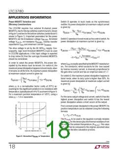
To prevent maximum junction temperature from being
exceeded, the input supply current must be checked
operating in continuous mode at maximum V .
In boost mode, when the FCB pin voltage is 0.85 < V
FCB
< 5.3V, the converter operates in Burst Mode operation.
In this mode, the controller clamps the peak inductor
current to approximately 20% of the maximum inductor
current. The output voltage ripple can increase during
Burst Mode operation.
IN
3780fe
19

 Linear Systems [ Linear Systems ]