2
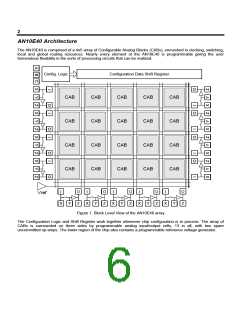
AN10E40 Architecture
The AN10E40 is comprised of a 4x5 array of Configurable Analog Blocks (CABs), enmeshed in clocking, switching,
local and global routing resources. Nearly every element of the AN10E40 is programmable giving the user
tremendous flexibility in the sorts of processing circuits that can be realized.
Config. Logic
Configuration Data Shift Register
CAB
CAB
CAB
CAB
CAB
CAB
CAB
CAB
CAB
CAB
CAB
CAB
CAB
CAB
CAB
CAB
CAB
CAB
CAB
CAB
I
O
Z
I
O
Z
I
O
Z
I
O
Z
I
O
Z
Vref
X
Y
X
Y
X
Y
X
Y
X
Y
Figure 1. Block Level View of the AN10E40 array
The Configuration Logic and Shift Register work together whenever chip configuration is in process. The array of
CABs is surrounded on three sides by programmable analog input/output cells, 13 in all, with two spare
uncommitted op-amps. The lower region of the chip also contains a programmable reference voltage generator.

 LATTICE [ LATTICE SEMICONDUCTOR ]