AN10E40 Data Manual
i
Table of Contents
Features of AN10E40................................................................................................................................................ 1
Available IPmodule Functions................................................................................................................................... 1
How It Works............................................................................................................................................................. 1
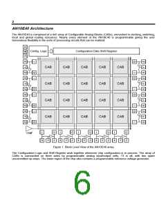
AN10E40 Architecture............................................................................................................................................... 2
The Configurable Analog Block ................................................................................................................................ 3
A Quick Review of Switched Capacitor Circuits.................................................................................................... 3
CAB Details ........................................................................................................................................................... 4
Routing Resources.................................................................................................................................................... 4
Clock Generation ...................................................................................................................................................... 4
Voltage Reference .................................................................................................................................................... 5
Voltage Mid-Rail Generator....................................................................................................................................... 5
Analog Input Output Cell........................................................................................................................................... 6
Sallen Key Filtering................................................................................................................................................ 6
2nd Order Sallen-Key Filter for Output Smoothing................................................................................................. 7
4th Order Sallen-Key Filter for Output Smoothing ................................................................................................. 7
2nd Order Sallen-Key Filter for Input Anti-Aliasing................................................................................................. 7
4th Order Sallen-Key Filter for Input Anti-Aliasing ................................................................................................. 8
Configuration Engine................................................................................................................................................. 9
Mode 0 – Micro Mode.......................................................................................................................................... 10
Micro Mode Configuration Sequence .............................................................................................................. 13
Micro Mode Maximum Data Transfer Rate...................................................................................................... 13
Mode 1 – Boot from ROM (BFR Mode)............................................................................................................... 14
BFR Timing.......................................................................................................................................................... 15
Configuration Clock ............................................................................................................................................. 16
Reset Sequences.................................................................................................................................................... 17
Analog Power On Reset (APOR) & Power On Reset (POR).............................................................................. 17
Internal Reset Activity.......................................................................................................................................... 17
External Reset Assertion..................................................................................................................................... 17
Mechanical.............................................................................................................................................................. 17
Package Details................................................................................................................................................... 17
Pin Out Description.............................................................................................................................................. 18
Package Pin Electrical Characterization................................................................................................................. 21
Powers, Grounds and Bypassing............................................................................................................................ 21
Recommended Configuration for Power & Ground............................................................................................. 21
AVDD and AVSS................................................................................................................................................. 21
SVDD and SVSS................................................................................................................................................. 21
BVDD and BVSS................................................................................................................................................. 22
ESD_VDD and ESD_VSS................................................................................................................................... 22
CFG_VDD and CFG_VSS .................................................................................................................................. 22
OPAMVMR and CEXT ........................................................................................................................................ 22
The AN10E40 in Split Supply Systems............................................................................................................... 22
Electrical Parameters.............................................................................................................................................. 22
Absolute Maximum Ratings................................................................................................................................. 23
Recommended Operating Conditions ................................................................................................................. 23
Digital IO.............................................................................................................................................................. 23
Voltage Mid Rail .................................................................................................................................................. 23
Vref ...................................................................................................................................................................... 23
The Analog I/O Cell ............................................................................................................................................. 24
The Analog I/O Cell Configured as a Sallen-Key Filter....................................................................................... 25
A Programmable Inverting Gain Stage................................................................................................................ 26
A Programmable Low Pass Filter........................................................................................................................ 27
Sine Wave Oscillator ........................................................................................................................................... 28
Electrostatic Discharge Characterization................................................................................................................ 28
A Quick Review of ESD Basics........................................................................................................................... 28
Catastrophic Failure......................................................................................................................................... 28
Latent Defect.................................................................................................................................................... 28

 LATTICE [ LATTICE SEMICONDUCTOR ]