AN10E40 Data Manual
1
Features of AN10E40
•
•
•
•
•
20 Programmable Analog Cells
13 Analog IO Cells
•
•
•
•
•
Easy Power-On-Reset Self Boot Using Serial PROM
Microprocessor Boot Option
Intuitive Design Software
2 Spare Op-Amps
8 Bit Programmable Internal Vref Source
4 Programmable Internal Clock Sources
Drift Free Designs
Rapidly Configurable
Available IPmodule Functions
•
•
•
•
•
•
•
•
Gain Stages
•
•
•
•
•
•
•
•
Non/Inverting Comparators
1 and 2 Input Comparators
DC Reference Voltage Sources
Limiters
Summing Amplifiers
Sample and Hold
Track and Hold
High, Low and Band Pass/Stop Filters
High Q, Low Q Filters
Cosine Filters
Schmitt Triggers
Non/Inverting Integrators
Differentiators
Full and Half Non/Inverting Rectifiers
New IP Modules Continuously Available
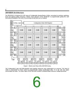
How It Works
On power up, the AN10E40’s reset circuitry initializes the configuration engine. The configuration engine takes over
and first examines the state of the Mode port. The pin settings of the Mode port determine which of the boot
methods should be exercised. One popular option is to boot from an off chip Serial PROM. The configuration
engine takes care of taking data out of the Serial PROM and loading it into on-chip configuration SRAM. The whole
boot process takes just a few milliseconds. Once the configuration SRAM has been loaded, the analog circuitry is
automatically enabled and the configuration engine idled. The chip now performs the analog functions according to
the configuration bit stream just loaded.
Creating a configuration bit stream is no more complicated than using the device itself. The AnadigmDesigner
design tool provides the user an intuitive drag and drop GUI in which you simply select several of the IPmodule
functions from the extensive library, drop them onto a graphical representation of the chip, fill in some parametric
information about the IPmodule, wire up the internal and I/O connections, and hit a button to generate the bit
stream (or download it directly to the device on your bench).
The device internals are more complicated than the easy to use device may lead you to believe. The AN10E40
array is based on programmable switched capacitor op-amp cells with very flexible internal and external connection
and clocking resources. The AnadigmDesigner and the associated IPmodule library shields the user from these
complexities.
Switched capacitor circuits are remarkably stable over voltage, temperature and device aging. Using the AN10E40
for your analog circuit realization allows you to rest assured knowing that once a circuit has been designed, it will
continue perform as expected. Say goodbye to trim pots.
Another advantage of this technology is the tremendous decrease in design time. Along with the elimination of trim
pots, you’ll also be able to clear your bench of all the normal discrete R and C components. “Prototyping” is now a
drag and drop computer exercise. A simple push of a button and your design is downloaded into the AN10E40
nearly instantaneously.
The kicker to all of this is that it is infinitely re-programmable. If a single set of analog functions is not sufficient for
your system, then you can load new configuration files into the AN10E40 with only a very small interruption to the
analog signal stream. Consider how filter parameters can be changed to adapt to varying input signal conditions.
Consider how a single physical circuit can be used in all of your different system designs. Consider all the
advantages that programmable analog will bring to your designs.

 LATTICE [ LATTICE SEMICONDUCTOR ]