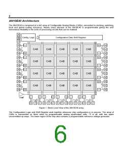
4
CAB Details
The SRAM block which controls routing connections and CAB behavior is loaded during configuration time.
Configuration typically occurs at power up as an automatic process but can of course be re-initiated at any time.
The ability to re-configure the part at any time gives the user incredible flexibility in system design.
Programmable capacitor banks and local switching in both the input paths to the op-amp and a programmable
capacitor bank in the op-amp’s feedback path provide all the resources required to realize a very large number of
analog processing circuits.
Global Outputs
Local Outputs
OpAmp
Global In
Configuration Memory (SRAM)
Figure 3. Block Level View of the basic CAB
Connection between other CAB’s on the device and to the outside world are accomplished using the Local Inputs,
Local Output, and Global routing resources.
Routing Resources
The most expedient way to gain understanding of the routing resources available on the AN10E40 is to use the
associated AnadigmDesigner design software. The routing resources and your connections to them are
represented in an intuitively obvious fashion.
Local routing resources are only shown (as fly lines or rubber band lines) in the design software screen once they
are used. A CAB output may be connected to an input in any of its 8 adjacent neighbors, and additionally to the
CAB in the same row and to the right two locations.
Global routing resources allow you to move signals to disparate locations on the die. There are a total of 10
horizontal global routes and 12 vertical global routes within the array. A CAB’s output can be connected to either of
the two adjacent right or two adjacent down global routes. A CAB’s input can be driven by one of the two adjacent
right or adjacent down global routes (which one of these two routes alternates with location in the array).
Connections to the chip’s programmable reference voltage generator are only available using Global routing
resources.
Clock Generation
Recall from the discussion on switched capacitor basics that the behavior of our simple circuit was influenced by
both the value of the capacitor as well as the frequency of the clock. So it is with IPmodules placed into the CABs of
the AN10E40 array. IPmodule input clocks are all derived from the master CLOCK input pin. The maximum rated
frequency of this input is currently specified to be 20 MHz. The master clock is split into 4 pairs of non-overlapping
clocks and bussed to each of the CABs. CLOCK[3:0] are derived from the dividing the master CLOCK input down
by a factor of 1 or from 2 to 62 (in increments of two). The maximum allowable clock frequency into an IPmodule is

 LATTICE [ LATTICE SEMICONDUCTOR ]