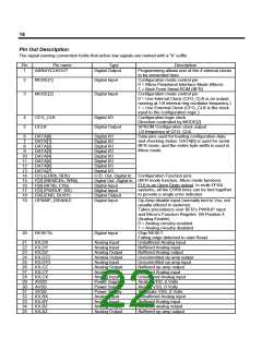
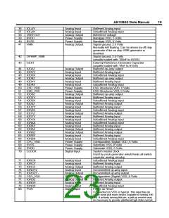
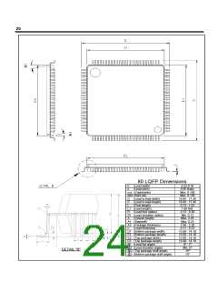
22
BVDD and BVSS
BVDD and BVSS supply all the band-gap voltage references, VMR generator and bias current generators. Here
again, the typical connection is to AVDD and AVSS.
ESD_VDD and ESD_VSS
These two signals do not normally source or sink any current to the AN10E40. In the rare event that a device pin is
electrically overstressed by an ESD or EOS event (Electrostatic Discharge or Electrical Overstress), then current is
sourced or sunk though these rails. These two should be connected to quiet supplies and here again AVDD and
AVSS are the typical connections.
CFG_VDD and CFG_VSS
The CFG_VDD and CFG_VSS rails supply all the digital configuration circuitry, the on board ring oscillator, APOR
and POR generation circuitry with +5V and 0V respectively. With the possible exception of the on board ring
oscillator, any digital supply noise produced by this circuitry would not normally effect the performance of the
analog portion, so no particular care need be taken with these supply signals from the chip’s point of view. Your
system however may have both “noisy” and “clean” power rails available. If so, CFG_Vxx may be best connected
to the “noisy” rail, leaving the “clean” supply as unpolluted as possible.
OPAMVMR and CEXT
As mentioned above in the Voltage Mid-Rail Generator section, both OPAMPVMR and CEXT should be bypassed
to a quiet ground node to ensure optimal performance. Generally, a good configuration consists of a Polyester
(Mylar) 10nF capacitor between CEXT and AVSS. A similar bypassing connection for OPAMPVMR is also
recommended. Care should be exercised in the placement of these components to minimize the signal path
between the array and the bypass capacitors.
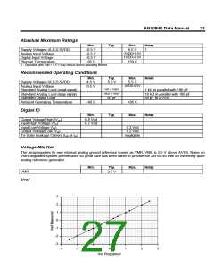
The AN10E40 in Split Supply Systems
All analog signal processing within the AN10E40 is
+2.5 V
referenced to its internal VMR node (Voltage Mid Rail,
normally 2.5 V above AVSS). For those applications
where a split supply (±2.5 V) is necessary, it is
VDD
possible to connect the AN10E40 as shown in Figure
20.
Analog
AN10E40
Interface
Ground
Referenced
Analog
Here the AN10E40's internal VMR generator is
disabled (a feature available via AnadigmDesigner)
and the chip's VMR pin is instead driven externally by
the system's ground plane.
Boot
VMR
PROM
(or Micro)
System
Naturally, logic circuits which interface to the AN10E40
must also be powered off the split rail as shown.
VSS
Under some circumstances, it may be more practical
to instead power the AN10E40 off a single 5 V supply
and AC coupled the ground referenced input signal.
-2.5 V
Figure 20. Connecting to a Split Rail System
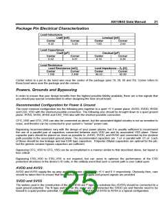
Electrical Parameters
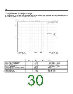
Because the AN10E40 is programmable, performance characteristics are reported for representative pieces of the
device rather than for the entire device. The following graphs and numbers provide you with conservative estimates
of the sort of performance you can expect for your particular design.

 LATTICE [ LATTICE SEMICONDUCTOR ]