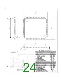
24
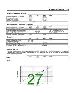
The Analog I/O Cell
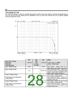
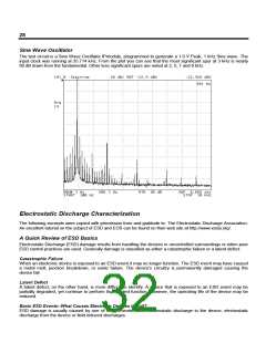
The AN10E40 Analog I/O cells are carefully designed to provide robust drive without sacrificing bandwidth figures.
You can see from the plot below that the bandwidth of the I/O cells well exceeds the sort of signals typically
processed within the device.
Min.
Typ.
2 mV
Max.
Notes
Input Offset Voltage
Unity Gain
-0.02 dB
0 dB
+0.02 dB 1 kHz, Sine, 1.0 VRMS
Slew Rate
10 kΩ , 100 pF load
20 V/µs
10.8 MHz
-3dB Bandwidth
Input Voltage Range
AVSS
0.5
AVDD
Pins IOxxZ - When used as a
direct input to the device core cells.
Pins IOxxX and IOxxY - When the
I/O cell is used as a powered input
buffer. (Input range is limited by I/O
buffer output swing limitations.)
Pins IOxxZ - When I/O cell is used
as a powered output buffer.
Input Voltage Range
AVDD- 0.5
Output Voltage Range
AVDD- 0.5
AVDD- 0.5
0.5
0.5
Small Signal Load Defined as:
1 k9|| 100 pF
Pins IOxxX and IOxxY - When I/O
cell is used as a direct output from
a device core cell.
Output Voltage Range
Pins IOxxZ - When I/O cell is used
as a powered output buffer.
Large Signal Load Defined as:
10 k9|| 100 pF
Pins IOxxX and IOxxY - When I/O
cell is used as a direct output from
a device core cell.

 LATTICE [ LATTICE SEMICONDUCTOR ]