LANSDALE Semiconductor, Inc.
ML145155
ML145155
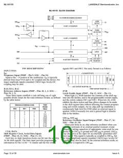
OUTPUT PINS
phase and frequency). LD pulses low when loop is out of lock.
PD
out
Phase Detector A Output (PDIP, SOG – Pin 6)
Three–state output of phase detector for use as loop error
signal. Double–ended outputs are also available for this pur-
pose (see φV and φR).
SW1, SW2
Band Switch Outputs (PDIP – Pins 13, 14; SOG – Pins 14, 15)
SW1 and SW2 provide latched open–drain outputs corre-
sponding to data bits numbers one and two. These outputs can
be tied through external resistors to voltages as high as 15 V,
Frequency f > f or f Leading: Negative Pulses
V
V
R
V
V
Frequency f < f or f Lagging: Positive Pulses
independent of the V
supply voltage. These are typically
R
DD
Frequency f = f and Phase Coincidence: High–Imped-
used for band switch functions. A logic 1 causes the output to
assume a high–impedance state, while a logic 0 causes the out-
put to be low.
V
R
ance State
φR, φV
Phase Detector B Outputs (PDIP, SOG – Pins 4, 3)
REF
out
These phase detector outputs can be combined externally for
a loop–error signal. A single–ended output is also available for
Buffered Reference Oscillator Output (PDIP, SOG – Pin 15)
Buffered output of on–chip reference oscillator or externally
provided reference–input signal.
this purpose (see PD ).
out
If frequency f is greater than f or if the phase of f is
V
R
V
leading, then error information is provided by f pulsing low.
POWER SUPPLY
V
f remains essentially high.
R
If the frequency f is less than f or if the phase of f is
VDD
V
R
V
lagging, then error information is provided by f pulsing low.
Positive Power Supply (PDIP, SOG – Pin 5)
The positive power supply potential. This pin may range
R
f
remains essentially high.
V
If the frequency of f = f and both are in phase, then both
from + 3 to + 9 V with respect to V
.
V
R
SS
f
and f remain high except for a small minimum time peri-
V
R
od when both pulse low in phase.
VSS
Negative Power Supply (PDIP, SOG – Pin 7)
The most negative supply potential. This pin is usually
ground.
LD
Lock Detector Output (PDIP – Pin 8, SOG – Pin 9)
Essentially a high level when loop is locked (f , f of same
R V
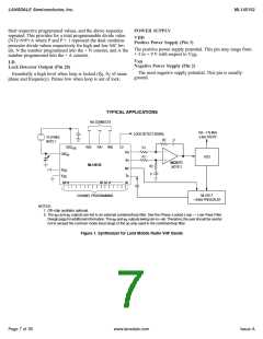
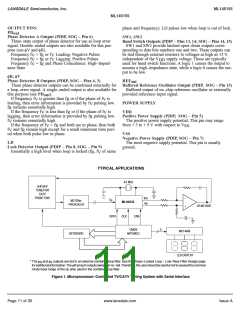
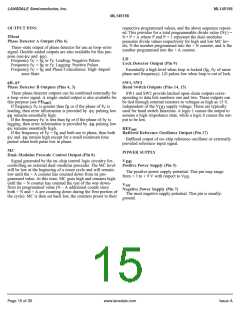
TYPICAL APPLICATIONS
4.0 MHz
UHF/VHF
TUNER OR
CATV
φ
FRONT END
–
+
R
f
in
MC120xx
PRESCALER
ML145155
φ
V
1/2 MC1458*
DATA
CLK
ENB
CMOS
MPU/MCU
3
MC14489
KEYBOARD
LED DISPLAY
* The φ and φ outputs are fed to an external combiner/loop filter. See the Phase–Locked Loop – Low–Pass Filter Design page
R
V
foradditionalinformation.TheφRandφVoutputsswingrail–to–rail.Therefore,theusershouldbecarefulnottoexceedthecommon
mode input range of the op amp used in the combiner/loop filter.
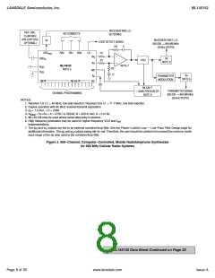
Figure 1. Microprocessor–Controlled TV/CATV Tuning System with Serial Interface
Page 11 of 35
www.lansdale.com
Issue A

 LANSDALE [ LANSDALE SEMICONDUCTOR INC. ]