LANSDALE Semiconductor, Inc.
ML145152
POWER SUPPLY
their respective programmed values, and the above sequence
repeated. This provides for a total programmable divide value
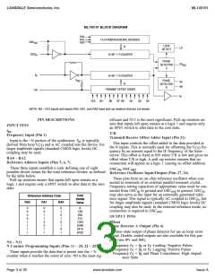
(NT)=N•P+A where P and P + 1 represent the dual–modulus
prescaler divide values respectively for high and low MC lev-
els, N the number programmed into the ÷ N counter, and A the
number programmed into the ÷ A counter.
VDD
Positive Power Supply (Pin 3)
The positive power supply potential. This pin may range from
+ 3 to + 9 V with respect to V
.
SS
V
SS
Negative Power Supply (Pin 2)
LD
Lock Detector Output (Pin 28)
The most negative supply potential. This pin is usually-
ground.
Essentially a high level when loop is locked (f , f of same
R V
phase and frequency). Pulses low when loop is out of lock.
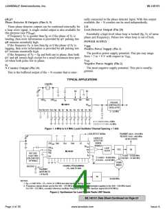
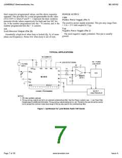
TYPICAL APPLICATIONS
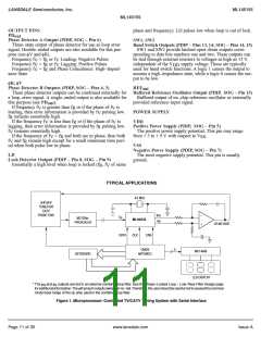
NO CONNECTS
“1”
“1”
“1”
150 – 175 MHz
5 kHz STEPS
LOCK DETECT SIGNAL
R2
10.24 MHz
NOTE 1
C
OSC
out
RA2
RA1
RA0
LD
R1
R1
φ
–
+
R
OSC
in
VCO
φ
V
MC33171
NOTE 2
ML145152
R2
C
MC
V
V
+ V
DD
f
in
SS
N9
N0 A5
A0
ML12017
CHANNEL PROGRAMMING
÷
64/65 PRESCALER
NOTES:
1. Off–chip oscillator optional.
2. The φ and φ outputs are fed to an external combiner/loop filter. See the Phase–Locked Loop — Low–Pass Filter
R
V
Design page for additional information. The φ and φ outputs swing rail–to–rail. Therefore, the user should be careful
R
V
not to exceed the common mode input range of the op amp used in the combiner/loop filter.
Figure 1. Synthesizer for Land Mobile Radio VHF Bands
Page 7 of 35
www.lansdale.com
Issue A

 LANSDALE [ LANSDALE SEMICONDUCTOR INC. ]