ML145155
LANSDALE Semiconductor, Inc.
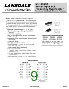
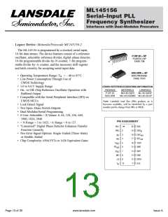
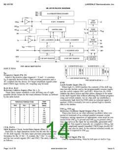
ML145155 BLOCK DIAGRAM
RA2
14 x 8 ROM REFERENCE DECODER
RA1
RA0
LOCK
DETECT
14
OSC
REF
out
LD
OSC
14–BIT
14–BIT
÷
÷
R COUNTER
in
f
PHASE
DETECTOR
A
R
PD
out
f
V
out
f
in
R COUNTER
14
PHASE
DETECTOR
B
φ
φ
V
R
V
DD
SW2
SW1
ENB
LATCH
LATCH
14
14–BIT SHIFT REGISTER
DATA
CLK
2–BIT SHIFT
REGISTER
PIN DESCRIPTIONS
signals SW1 and SW2. The entry format is as follows:
INPUT PINS
in
f
÷
N COUNTER BITS
Frequency Input (PDIP – Pin 9, SOG – Pin 10)
Input to the ÷ N portion of the synthesizer. f is typically
in
derived from loop VCO and is AC coupled into the device. For
larger amplitude signals (standard CMOS logic levels) DC
coupling may be used.
LAST DATA BIT IN (BIT NO. 16)
FIRST DATA BIT IN (BIT NO. 1)
RA0, RA1, RA2
Reference Address Inputs (PDIP – Pins 18, 1, 2; SOG –
Pins 20, 1, 2)
These three inputs establish a code defining one of eight
possible divide values for the total reference divider, as defined
by the table below:
ENB
Latch Enable Input (PDIP – Pin 12, SOG – Pin 13)
When high (1), ENB transfers the contents of the shift reg-
ister into the latches, and to the programmable counter inputs,
and the switch outputs SW1 and SW2. When low (0), ENB
inhibits the above action and thus allows changes to be made
in the shift register data without affecting the counter program-
ming and switch outputs. An on–chip pull–up establishes a
continuously high level for ENB when no external signal is
applied. ENB is normally low and is pulsed high to transfer
data to the latches.
Total
Divide
Value
Reference Address Code
RA2
RA1
RA0
0
0
0
0
1
1
1
1
0
0
1
1
0
0
1
1
0
1
0
1
0
1
0
1
16
512
1024
2048
3668
4096
6144
8192
OSC , OSC
in out
Reference Oscillator Input/Output (PDIP – Pins 17, 16;
SOG – Pins 19, 18)
These pins form an on–chip reference oscillator when con-
nected to terminals of an external parallel resonant crystal.
Frequency setting capacitors of appropriate value must be con-
CLK, DATA
Shift Register Clock, Serial Data Inputs
(PDIP – Pins 10, 11; SOG – Pins 11, 12)
Each low–to–high transition clocks one bit into the on–chip
16–bit shift register. The Data input provides programming
information for the 14–bit ÷ N counter and the two switch
nected from OSC to ground and OSC
to ground. OSC
in out
in
may also serve as the input for an externally–generated refer-
ence signal. This signal is typically ac coupled to OSC , but
in
for larger amplitude signals (standard CMOS logic levels) DC
coupling may also be used. In the external reference mode, no
connection is required to OSC
.
out
Page 10 of 35
www.lansdale.com
Issue A

 LANSDALE [ LANSDALE SEMICONDUCTOR INC. ]