LANSDALE Semiconductor, Inc.
ML145152
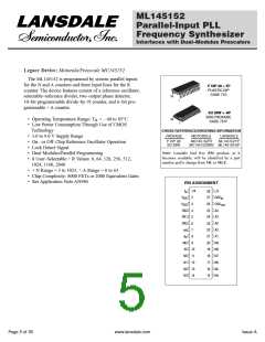
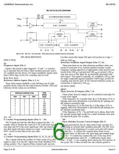
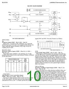
ML145152 BLOCK DIAGRAM
RA2
RA1
RA0
12 x 8 ROM REFERENCE DECODER
12
OSC
out
LOCK
DETECT
LD
OSC
in
12–BIT
÷
R COUNTER
MC
φ
φ
V
CONTROL
LOGIC
PHASE
DETECTOR
R
f
in
6–BIT
A5
÷
A COUNTER
10–BIT
N2
÷
N COUNTER
A3 A2
A0
N0
N4 N5
N7
N9
NOTE: N0 – N9, A0 – A5, and RA0 – RA2 have pull–up resistors that are not shown.
PIN DESCRIPTIONS
tors that ensure that inputs left open will remain at a logic 1.
INPUT PINS
OSC , OSC
in
out
Reference Oscillator Input/Output (Pins 27, 26)
f
in
Frequency Input (Pin 1)
These pins form an on–chip reference oscillator when con-
nected to terminals of an external parallel resonant crystal.
Frequency setting capacitors of appropriate value must be con-
Input to the positive edge triggered ÷ N and ÷ A counters.
f
is typically derived from a dual–modulus prescaler and is
in
nected from OSC to ground and OSC
to ground. OSC
in out
in
AC coupled into the device. For larger amplitude signals (stan-
dard CMOS logic levels) DC coupling may be used.
may also serve as the input for an externally generated refer-
ence signal. This signal is typically AC coupled to OSC , but
in
RA0, RA1, RA2
Reference Address Inputs (Pins 4, 5, 6)
for larger amplitude signals (standard CMOS logic levels) DC
coupling may also be used. In the external reference mode, no
connection is required to OSC
OUTPUT PINS
φR,φV
.
These three inputs establish a code defining one of eight
possible divide values for the total reference divider. The total
reference divide values are as follows:
out
Phase Detector B Outputs (Pins 7, 8)
Total
Divide
Value
Reference Address Code
These phase detector outputs can be combined externally for
a loop–error signal.
If the frequency f is greater than f or if the phase of f is
leading, then error information is provided by φV pulsing low.
φR remains essentially high.
If the frequency f is less than f or if the phase of f is
RA2
RA1
RA0
V
R
V
0
0
0
0
1
1
1
1
0
0
1
1
0
0
1
1
0
1
0
1
0
1
0
1
8
64
128
256
512
1024
1160
2048
V
R
V
lagging, then error information is provided by φR pulsing low.
φV remains essentially high.
If the frequency of f = f and both are in phase, then both
V
R
φV and φR remain high except for a small minimum time peri-
od when both pulse low in phase.
N0 – N9
N Counter Programming Inputs (Pins 11 – 20)
MC
Dual–Modulus Prescale Control Output (Pin 9)
The N inputs provide the data that is preset into the ÷ N
counter when it reaches the count of 0. N0 is the least signifi-
cant digit and N9 is the most significant. Pull–up resistors en-
sure that inputs left open remain at a logic 1 and require only a
SPST switch to alter data to the zero state.
Signal generated by the on–chip control logic circuitry for
controlling an external dual–modulus prescaler. The MC level
will be low at the beginning of a count cycle and will remain
low until the ÷ A counter has counted down from its pro-
grammed value. At this time, MC goes high and remains high
until the ÷ N counter has counted the rest of the way down
from its programmed value (N – A additional counts since
both ÷ N and ÷ A are counting down during the first portion of
the cycle). MC is then set back low, the counters preset to
A0 – A5
A Counter Programming Inputs(Pins 23, 21, 22, 24, 25, 10)
The A inputs define the number of clock cycles of f that
in
require a logic 0 on the MC output (see Dual–Modulus Pres-
caling section). The A inputs all have internal pull–up resis-
Page 6 of 35
www.lansdale.com
Issue A

 LANSDALE [ LANSDALE SEMICONDUCTOR INC. ]