ISL88731C
Signal Ground and Power Ground
Connection
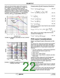
S E N S E
E S IS T O
H
R
T R A C
IG
R
H
E N
H
R
IG
R
H
E N T
R
R
C
U
T
C
U
E
T R A C E
At minimum, a reasonably large area of copper, which
will shield other noise couplings through the IC, should
be used as signal ground beneath the IC. The best
tie-point between the signal ground and the power
ground is at the negative side of the output capacitor on
each side, where there is little noise; a noisy trace
beneath the IC is not recommended.
K E L V IN C O
T O T H E L O
S O
N
W
P
N E C T IO
P A S S F IL T E R A N D
A N S O
N T R A C E S
C
D
C
N
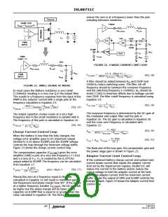
FIGURE 28. CURRENT SENSE RESISTOR LAYOUT
CSOP, CSON, CSSP and CSSN Pins
GND and VCC Pin
Accurate charge current and adapter current sensing is
critical for good performance. The current sense resistor
connects to the CSON and the CSOP pins through a low
pass filter with the filter capacitor very near the IC (see
Figure 4). Traces from the sense resistor should start at
the pads of the sense resistor and should be routed close
together, through the low pass filter and to the CSOP and
CSON pins (see Figure 28). The CSON pin is also used as
the battery voltage feedback. The traces should be
routed away from the high dv/dt and di/dt pins like
PHASE, BOOT pins. In general, the current sense resistor
should be close to the IC. These guidelines should also be
followed for the adapter current sense resistor and CSSP
and CSSN. Other layout arrangements should be
adjusted accordingly.
At least one high quality ceramic decoupling capacitor
should be used to cross these two pins. The decoupling
capacitor can be put close to the IC.
LGATE Pin
This is the gate drive signal for the bottom MOSFET of
the buck converter. The signal going through this trace
has both high dv/dt and high di/dt, and the peak
charging and discharging current is very high. These two
traces should be short, wide, and away from other
traces. There should be no other traces in parallel with
these traces on any layer.
PGND Pin
PGND pin should be laid out to the negative side of the
relevant output capacitor with separate traces.The
negative side of the output capacitor must be close to the
source node of the bottom MOSFET. This trace is the
return path of LGATE.
DCIN Pin
This pin connects to AC-adapter output voltage, and
should be less noise sensitive.
Copper Size for the Phase Node
PHASE Pin
The capacitance of PHASE should be kept very low to
minimize ringing. It would be best to limit the size of the
PHASE node copper in strict accordance with the current
and thermal management of the application.
This trace should be short, and positioned away from
other weak signal traces. This node has a very high dv/dt
with a voltage swing from the input voltage to ground.
No trace should be in parallel with it. This trace is also the
return path for UGATE. Connect this pin to the high-side
MOSFET source.
Identify the Power and Signal Ground
The input and output capacitors of the converters, the
source terminal of the bottom switching MOSFET PGND
should connect to the power ground. The other
components should connect to signal ground. Signal and
power ground are tied together at one point.
UGATE Pin
This pin has a square shape waveform with high dv/dt. It
provides the gate drive current to charge and discharge
the top MOSFET with high di/dt. This trace should be
wide, short, and away from other traces, similar to the
LGATE.
Clamping Capacitor for Switching MOSFET
It is recommended that ceramic capacitors be used
closely connected to the drain of the high-side MOSFET,
and the source of the low-side MOSFET. This capacitor
reduces the noise and the power loss of the MOSFET.
BOOT Pin
This pin’s di/dt is as high as the UGATE; therefore, this
trace should be as short as possible.
FN6978.0
March 8, 2010
23

 INTERSIL [ Intersil ]