ICL7116, ICL7117
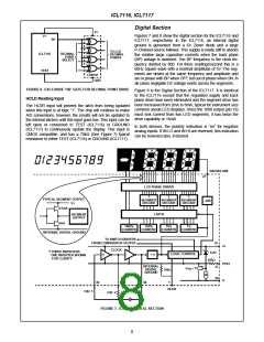
Digital Section
V+
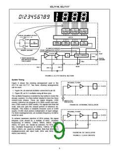
Figures 7 and 8 show the digital section for the ICL7116 and
ICL7117, respectively. In the ICL7116, an internal digital
ground is generated from a 6V Zener diode and a large
P-Channel source follower. This supply is made stiff to absorb
the relative large capacitive currents when the back plane
(BP) voltage is switched. The BP frequency is the clock fre-
quency divided by 800. For three readings/second this is a
60Hz square wave with a nominal amplitude of 5V. The seg-
ments are driven at the same frequency and amplitude and
are in phase with BP when OFF, but out of phase when ON. In
all cases negligible DC voltage exists across the segments.
V+
BP
TO LCD
DECIMAL
POINTS
ICL7116
TEST
DECIMAL
POINT
SELECT
CD4030
GND
FIGURE 6. EXCLUSIVE ‘OR’ GATE FOR DECIMAL POINT DRIVE
HOLD Reading Input
Figure 8 is the Digital Section of the ICL7117. It is identical
to the ICL7116 except that the regulated supply and back
plane drive have been eliminated and the segment drive has
been increased from 2mA to 8mA, typical for instrument size
common anode LED displays. Since the 1000 output (pin 19)
must sink current from two LED segments, it has twice the
drive capability or 16mA.
The HLDR input will prevent the latch from being updated
when this input is at logic “1”. The chip will continue to make
A/D conversions, however, the results will not be updated to
the internal latches until this input goes low. This input can be
left open or connected to TEST (ICL7116) or GROUND
(ICL7117) to continuously update the display. This input is
CMOS compatible, and has a 70kΩ (See Figure 7) typical
resistance to either TEST (ICL7116) or GROUND (ICL7117).
In both devices, the polarity indication is “on” for negative
analog inputs. If IN LO and IN HI are reversed, this indication
can be reversed also, if desired.
a
a
a
f
f
f
a
b
b
b
g
g
g
c
e
e
e
c
c
c
b
d
d
d
BACKPLANE
21
LCD PHASE DRIVER
7
7
7
TYPICAL SEGMENT OUTPUT
V+
SEGMENT
DECODE
SEGMENT
DECODE
SEGMENT
DECODE
÷200
0.5mA
LATCH
SEGMENT
OUTPUT
2mA
1000’s
100’s
10’s
1’s
COUNTER
COUNTER
COUNTER
COUNTER
INTERNAL DIGITAL GROUND
TO SWITCH DRIVERS
35
FROM COMPARATOR OUTPUT
V+
CLOCK
† THREE INVERTERS
ONE INVERTER SHOWN
FOR CLARITY
6.2V
500Ω
LOGIC CONTROL
÷
4
†
TEST
V-
INTERNAL
DIGITAL
37
V
= 1V
TH
70kΩ
GROUND
26
40
39
38
1
HLDR
OSC 1
OSC 3
OSC 2
FIGURE 7. ICL7116 DIGITAL SECTION
8

 INTERSIL [ Intersil ]