ICL7116, ICL7117
have a full scale reading when the voltage from the
transducer is 0.682V. Instead of dividing the input down to
200mV, the designer should use the input voltage directly
Component Value Selection
Integrating Resistor
and select V
= 0.341V. Suitable values for integrating
REF
Both the buffer amplifier and the integrator have a class A
output stage with 100µA of quiescent current. They can
supply 4µA of drive current with negligible nonlinearity. The
integrating resistor should be large enough to remain in this
very linear region over the input voltage range, but small
enough that undue leakage requirements are not placed on
the PC board. For 2V full scale, 470kΩ is near optimum and
similarly a 47kΩ for a 200mV scale.
resistor and capacitor would be 120kΩ and 0.22µF. This
makes the system slightly quieter and also avoids a divider
network on the input. The ICL7117 with ±5V supplies can
accept input signals up to ±4V. Another advantage of this
system occurs when a digital reading of zero is desired for
V
≠ 0. Temperature and weighing systems with a variable
IN
fare are examples. This offset reading can be conveniently
generated by connecting the voltage transducer between IN
HI and COMMON and the variable (or fixed) offset voltage
between COMMON and IN LO.
Integrating Capacitor
The integrating capacitor should be selected to give the
maximum voltage swing that ensures tolerance buildup will
not saturate the integrator swing (approximately. 0.5V from
either supply). In the ICL7116 or the ICL7117, when the
analog COMMON is used as a reference, a nominal +2V full-
scale integrator swing is fine. For the ICL7117 with +5V
supplies and analog COMMON tied to supply ground, a
±3.5V to +4V swing is nominal. For three readings/second
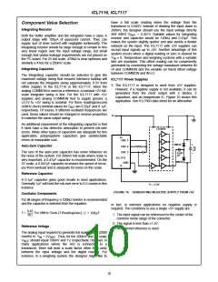
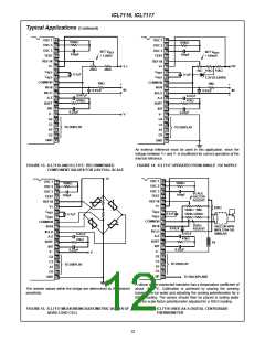
ICL7117 Power Supplies
3. The ICL7117 is designed to work from ±5V supplies.
However, if a negative supply is not available, it can be
generated from the clock output with 2 diodes, 2
capacitors, and an inexpensive lC. Figure 10 shows this
application. See ICL7660 data sheet for an alternative.
(48kHz clock) nominal values for C
are 0.22µF and 0.1µF,
lNT
respectively. Of course, if different oscillator frequencies are
used, these values should be changed in inverse proportion
to maintain the same output swing.
V+
An additional requirement of the integrating capacitor is that
it must have a low dielectric absorption to prevent roll-over
errors. While other types of capacitors are adequate for this
application, polypropylene capacitors give undetectable
errors at reasonable cost.
CD4009
V+
OSC 1
IN914
+
10
µF
-
Auto-Zero Capacitor
OSC 2
OSC 3
The size of the auto-zero capacitor has some influence on
the noise of the system. For 200mV full scale where noise is
very important, a 0.47µF capacitor is recommended. On the
2V scale, a 0.047µF capacitor increases the speed of recov-
ery from overload and is adequate for noise on this scale.
0.047
µF
ICL7117
GND
IN914
V-
Reference Capacitor
A 0.1µF capacitor gives good results in most applications.
Generally 1µF will hold the roll-over error to 0.5 counts in this
instance.
V- = 3.3V
FIGURE 10. GENERATING NEGATIVE SUPPLY FROM +5V
Oscillator Components
For all ranges of frequency a 100kΩ resistor is recommended
and the capacitor is selected from the equation:
In fact, in selected applications no negative supply is
required. The conditions to use a single +5V supply are:
0.45
------------
f =
For 48kHz Clock (3 Readings/sec),
C = 100pF.
1. The input signal can be referenced to the center of the
common mode range of the converter.
RC
2. The signal is less than ±1.5V.
Reference Voltage
The analog input required to generate full scale output (2000
3. An external reference is used.
counts) is: V = 2V
. Thus, for the 200mV and 2V scale,
lN REF
V
should equal 100mV and 1V, respectively. However, in
REF
many applications where the A/D is connected to a
transducer, there will exist a scale factor other than unity
between the input voltage and the digital reading. For
instance, in a weighing system, the designer might like to
10

 INTERSIL [ Intersil ]