ICL7116, ICL7117
output to return to zero is proportional to the input signal.
Specifically the digital reading displayed is:
Detailed Description
Analog Section
V
IN
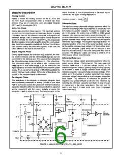
Figure 3 shows the Analog Section for the ICL7116 and
ICL7117. Each measurement cycle is divided into three
phases. They are (1) auto-zero (A-Z), (2) signal integrate
(INT) and (3) de-integrate (DE).
----------------
DISPLAY COUNT = 1000
.
V
REF
Differential Input
The input can accept differential voltages anywhere within the
common mode range of the input amplifier, or specifically from
0.5V below the positive supply to 1V above the negative sup-
ply. In this range, the system has a CMRR of 86dB typical.
However, care must be exercised to assure the integrator out-
put does not saturate. A worst case condition would be a large
positive common mode voltage with a near full scale negative
differential input voltage. The negative input signal drives the
integrator positive when most of its swing has been used up
by the positive common mode voltage. For these critical appli-
cations the integrator output swing can be reduced to less
than the recommended 2V full scale swing with little loss of
accuracy. The integrator output can swing to within 0.5V of
either supply without loss of linearity.
Auto-Zero Phase
During auto-zero three things happen. First, input high and low
are disconnected from the pins and internally shorted to analog
COMMON. Second, the reference capacitor is charged to the
reference voltage. Third, a feedback loop is closed around the
system to charge the auto-zero capacitor C to compensate
AZ
for offset voltages in the buffer amplifier, integrator, and compar-
ator. Since the comparator is included in the loop, the A-Z accu-
racy is limited only by the noise of the system. In any case, the
offset referred to the input is less than 10µV.
Signal Integrate Phase
During signal integrate, the auto-zero loop is opened, the inter-
nal short is removed, and the internal input high and low are
connected to the external pins. The converter then integrates
the differential voltage between IN HI and IN LO for a fixed time.
This differential voltage can be within a wide common mode
range: up to 1V from either supply. If, on the other hand, the
input signal has no return with respect to the converter power
supply, IN LO can be tied to analog COMMON to establish the
correct common mode voltage. At the end of this phase, the
polarity of the integrated signal is determined.
Differential Reference
The reference voltage can be generated anywhere within the
power supply voltage of the converter. The main source of
common mode error is a roll-over voltage caused by the
reference capacitor losing or gaining charge to stray capacity
on its nodes. If there is a large common mode voltage, the
reference capacitor can gain charge (increase voltage) when
called up to de-integrate a positive signal but lose charge
(decrease voltage) when called up to de-integrate a negative
input signal. This difference in reference for positive or
negative input voltage will give a roll-over error. However, by
selecting the reference capacitor such that it is large enough
in comparison to the stray capacitance, this error can be
held to less than 0.5 count worst case. (See Component
Value Selection.)
De-Integrate Phase
The final phase is de-integrate, or reference integrate. Input
low is internally connected to analog COMMON and input
high is connected across the previously charged reference
capacitor. Circuitry within the chip ensures that the capacitor
will be connected with the correct polarity to cause the
integrator output to return to zero. The time required for the
STRAY
STRAY
C
REF
R
C
C
INT
INT
AZ
BUFFER
REF HI
36
V+
35
C
+
C
-
A-Z
INT
27
REF
REF
34
33
28
29
V+
A-Z
INTEGRATOR
-
+
TO
DIGITAL
SECTION
10µA
-
+
+
2.8V
31
IN HI
DE-
DE+
INT
6.2V
A-Z
INPUT
HIGH
A-Z
COMPARATOR
A-Z
DE-
+
-
N
DE+
32
30
COMMON
IN LO
INPUT
LOW
A-Z AND DE(±)
INT
26
V-
FIGURE 3. ANALOG SECTION OF ICL7116 AND ICL711
6

 INTERSIL [ Intersil ]