ICL7116, ICL7117
Absolute Maximum Ratings
Thermal Information
o
Supply Voltage
Thermal Resistance (Typical, Note 2)
θJA ( C/W)
ICL7116, V+ to V- . . . . . . . . . . . . . . . . . . . . . . . . . . . . . . . . . . 15V
ICL7117, V+ to GND. . . . . . . . . . . . . . . . . . . . . . . . . . . . . . . . . 6V
ICL7117, V- to GND . . . . . . . . . . . . . . . . . . . . . . . . . . . . . . . . .-9V
Analog Input Voltage (Either Input) (Note 1). . . . . . . . . . . . . V+ to V-
Reference Input Voltage (Either Input) . . . . . . . . . . . . . . . . . V+ to V-
Clock Input
PDIP Package . . . . . . . . . . . . . . . . . . . . . . . . . . . . .
MQFP Package . . . . . . . . . . . . . . . . . . . . . . . . . . . .
Maximum Junction Temperature . . . . . . . . . . . . . . . . . . . . . . . 150 C
Maximum Storage Temperature Range . . . . . . . . . .-65 C to 150 C
Maximum Lead Temperature (Soldering 10s) . . . . . . . . . . . . . 300 C
50
80
o
o
o
o
(MQFP - Lead Tips Only)
ICL7116 . . . . . . . . . . . . . . . . . . . . . . . . . . . . . . . . . . . TEST to V+
ICL7117 . . . . . . . . . . . . . . . . . . . . . . . . . . . . . . . . . . . .GND to V+
Operating Conditions
o
o
Temperature Range . . . . . . . . . . . . . . . . . . . . . . . . . . . .0 C to 70 C
CAUTION: Stresses above those listed in “Absolute Maximum Ratings” may cause permanent damage to the device. This is a stress only rating and operation
of the device at these or any other conditions above those indicated in the operational sections of this specification is not implied.
NOTES:
1. Input voltages may exceed the supply voltages provided the input current is limited to ±100µA.
2. θ is measured with the component mounted on an evaluation PC board in free air.
JA
o
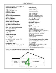
Electrical Specifications (Note 3) T = 25 C, f
= 48kHz, V
= 100mV
REF
A
CLOCK
PARAMETER
TEST CONDITIONS
MIN
TYP
MAX
UNITS
SYSTEM PERFORMANCE
Zero Input Reading
Ratiometric Reading
Rollover Error
V
V
= 0V, Full Scale = 200mV
-000.0 ±000.0 +000.0 Digital
IN
lN
Reading
= V
, V
REF REF
= 100mV
999
999/
1000
1000
±1
Digital
Reading
-V = +V
IN
195mV Difference in Reading for Equal
-
-
±0.2
Counts
lN
Positive and Negative Inputs Near Full Scale
Linearity
Full Scale = 200mV or Full Scale = 2V Maximum
Deviation from Best Straight Line Fit (Note 5)
±0.2
±1
Counts
Common Mode Rejection Ratio
Noise
V
V
= ±1V, V = 0V, Full Scale = 200mV (Note 5)
IN
-
-
50
15
-
-
µV/V
µV
CM
= 0V, Full Scale = 200mV (Peak-To-Peak Value
IN
Not Exceeded 95% of Time) (Note 5)
Leakage Current Input
V
V
V
V
= 0 (Note 5)
o
-
1
10
1
pA
lN
lN
IN
IN
o
o
Zero Reading Drift
= 0, 0 C To 70 C (Note 5)
-
0.2
1
µV/ C
o
o
o
Scale Factor Temperature Coefficient
V+ Supply Current
= 199mV, 0 C To 70 C (Note 5)
-
-
5
ppm/ C
= 0 (Does Not Include LED Current for ICL7117)
1.0
0.6
3.0
1.8
1.8
3.2
mA
mA
V
V- Supply Current
ICL7117 Only
-
COMMON Pin Analog Common Voltage
25kΩ Between Common and Positive Supply (With
2.4
Respect to + Supply)
o
Temperature Coefficient of Analog Common 25kΩ Between Common and Positive Supply (With
-
80
-
ppm/ C
Respect to + Supply) (Note 5)
DISPLAY DRIVER (ICL7116 ONLY)
Peak-To-Peak Segment Drive Voltage
Peak-To-Peak Backplane Drive Voltage
V+ = to V- = 9V, (Note 4)
4
5.5
6
V
DISPLAY DRIVER (ICL7117 ONLY)
Segment Sinking Current
(Except Pins 19 and 20)
V+ = 5V, Segment Voltage = 3V
5
10
4
8
16
7
-
-
-
mA
mA
mA
Pin 19 Only
Pin 20 Only
NOTES:
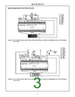
3. Unless otherwise noted, specifications apply to both the ICL7116 and ICL7117. ICL7116 is tested in the circuit of Figure 1. ICL7117 is
tested in the circuit of Figure 2.
4. Back plane drive is in phase with segment drive for ‘off’ segment, 180 degrees out of phase for ‘on’ segment. Frequency is 20 times con-
version rate. Average DC component is less than 50mV.
5. Not tested, guaranteed by design.
2

 INTERSIL [ Intersil ]