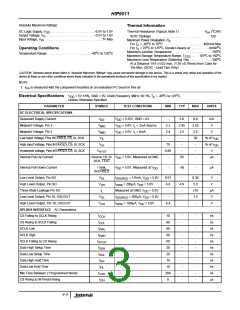
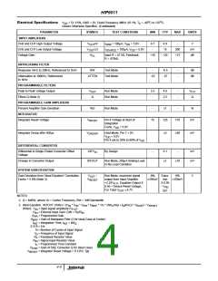
HIP9011
Programmable Gain Stage
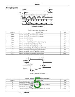
Circuit Block Description
The gains for two identical programmable gain stages can
be adjusted, so that the knock energies can be
compensated if needed. This adjustment can be made with
64 different gain settings, ranging between 2 and 0.111.
Input Amplifiers
Two amplifiers can be selected to interface to the engine
sensors. These amplifiers have a typical open loop gain of
100dB, with a typical bandwidth of 2.6MHz. The common
mode input voltage range extends to within 0.5V of either
supply rail. The amplifier output has a similar output range.
The signals can swing between 20 to 80 percent of V
.
DD
Programming is discussed in the SPI Communications
Protocol section.
Sufficient gain, bandwidth and output swing capability is
provided to ensure that the amplifier can handle
attenuation gain settings of 20 to 1 or -26dB. This would be
needed when high peak output signals, in the range of
Programmable Bandpass Filter
Two identical programmable filters are used to detect the
frequencies of interest. The Band Pass Filter (BPF) is
programmed to pass the frequency component of the engine
knock. The filter frequency is established by the characteristics
of the particular engine and transducer. By integrating the
rectified outputs from these two filters at the INTEGRATOR
stage, a knock can be detected if it has occurred.
8V
are obtained from the transducer. Gain settings of
RMS
10 times can also be needed when the transducers have
output levels of 5mV
.
RMS
In a typical application the input signal frequency may vary
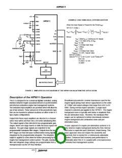
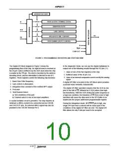
from 1kHz to 20kHz. External capacitors are used to
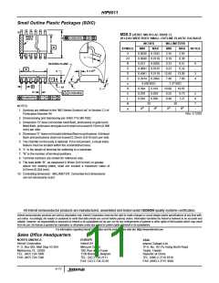
decouple the IC from the sensor (C1 and C2) refer to
Figure 4. A typical value of the capacitor would be 3.3nF.
Series input resistors, R1 and R2, are used to connect the
inverting inputs of the amplifiers, (pins 19 and 16.)
Feedback resistors, R3 and R4, in conjunction with R3 and
R4 are used to set the gain of the amplifiers.
The filters have a nominal differential gain of 4. Their
frequency is set by a programmable word (discussed in the
SPI Communications Protocol section.) Center frequencies
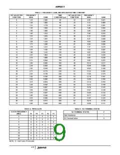
can be programed from 1.22kHz to 19.98kHz, in 64 steps.
The filter Qs are typically 2.4.
Active Full Wave Rectifier
The output of the bandpass filters are unity gain buffered prior
to full wave rectification using switch capacitor techniques.
Each side of the rectifier circuit provides both negative and
positive values of the knock frequency bandpass frequency
filter outputs. The output is able to swing from 20 to 80 percent
A mid voltage level is generated internally within the IC. This
level is set to be half way between V
and ground.
DD
Throughout the IC this level is used as a quiet, DC reference
for the signal processing circuits within the IC. This point is
brought out for several reasons, it can be used as a
reference voltage, and it must be bypassed to insure that it
remains as a quiet reference for the internal circuitry.
of V . Care was taken to minimize the RMS variations from
DD
input to output of this stage.
Programmable Integrator Stage
The input amplifiers are designed with power down
capability, which, when activated disables their bias circuit
and their output goes into a three-state state condition.
This is utilized during the diagnostic mode, in which the
output terminals of the amplifiers are driven by the outside
world with various test signals.
The signals from the rectifier stage are separated into 2 output
signal paths which are then integrated together. A differential
system is used to minimize noise. One side integrates the
positive energy value from the Knock Frequency Rectifier. The
second side does the integration of the negative energy value.
The positive and negative energy signals are opposite phase
signals. Using this technique reduces system noise from
affecting the actual signal.
Antialiasing Filter
The IC has a 3rd order Butterworth filter with a 3dB point at
70kHz. Double poly capacitors and implanted resistors are
used to set poles in the filter. This filter is required to have no
more than 1dB attenuation at 20kHz (highest frequency off
interest) and a minimum attenuation of 10dB at 180kHz. This
filter precedes the switch capacitor filter stages which run at
the system frequency of 200kHz.
The integrator time constant is software programmable by
the Integrator Time Constant discussed in the
Communications Protocol section. The time constant can be
programmed from 40µs to 600µs, with a total of 32 steps. If
for example, we program a time constant to 200µs, then with
one volt difference between each channel, the output of the
integrator will change by volt in 200µs.
R3
R4
C1
R1
C2
R2
19
20
16
15
-
-
18
17
SENSOR
SENSOR
+
+
VMID
VMID
FIGURE 4. INPUT AMPLIFIER CONNECTIONS
4-7

 INTERSIL [ Intersil ]