HIP9011
Absolute Maximum Ratings
DC Logic Supply, V . . . . . . . . . . . . . . . . . . . . . . . . . -0.5V to 7.0V
Thermal Information
o
Thermal Resistance (Typical, Note 1)
θ
( C/W)
DD
Output Voltage, V . . . . . . . . . . . . . . . . . . . . . . . . . . . -0.5V to 7.0V
JA
O
SOIC Package . . . . . . . . . . . . . . . . . . . . . . . . . . . . .
120
Input Voltage, V . . . . . . . . . . . . . . . . . . . . . . . . . . . . . . . . .7V Max
IN
Maximum Power Dissipation, P
D
o
o
For T = -40 C to 70 C . . . . . . . . . . . . . . . . . . . . . . .400mW Max
A
o
o
o
For T = 70 C to 125 C, Derate Linearly at . . . . . . . . . . 6mW/ C
Operating Conditions
A
o
Maximum Junction Temperature . . . . . . . . . . . . . . . . . . . . . . .150 C
Maximum Storage Temperature Range, T
Maximum Lead Temperature (Soldering 10s) . . . . . . . . . . . . .300 C
At a Distance 1/16 ±1/32 inch, (1.59 ±0.79mm) from Case for
10s Max. (SOIC - Lead Tips Only)
o
o
Temperature Range . . . . . . . . . . . . . . . . . . . . . . . . . -40 C to 125 C
o
o
. . . . -65 C to 150 C
STG
o
CAUTION: Stresses above those listed in “Absolute Maximum Ratings” may cause permanent damage to the device. This is a stress only rating and operation of the
device at these or any other conditions above those indicated in the operational sections of this specification is not implied.
NOTE:
1. θ is measured with the component mounted on an evaluation PC board in free air.
JA
o
o
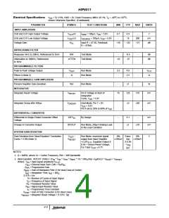
Electrical Specifications
V
= 5V ±5%, GND = 0V, Clock Frequency 4MHz ±0.1%, T = -40 C to 125 C,
DD A
Unless Otherwise Specified
PARAMETER
SYMBOL
TEST CONDITIONS
MIN
TYP
MAX
UNITS
DC ELECTRICAL SPECIFICATIONS
Quiescent Supply Current
I
V
V
V
V
V
= 5.25V, GND = 0V
-
2.3
2.4
-
5.0
2.45
2.5
-
8.0
2.55
2.6
30
-
mA
V
DD
DD
DD
DD
Midpoint Voltage, Pin 3
= 5.0V, I = 2mA Source
L
MID
MID
Midpoint Voltage, Pin 3
= 5.0V, I = 0mA
L
V
Low Input Voltage, Pins INT/HOLD, CS, SI, SCK
High Input Voltage, Pins INT/HOLD, CS, SI, SCK
Hysteresis voltage, Pins INT/HOLD, CS, SI, SCK
Internal Pull-Up Current
V
% of V
% of V
V
IL
DD
V
70
0.85
-
-
IH
DD
V
-
-
HYST
I Source CS, SI,
SCK, TEST
V
V
= 5.0V, Measured at GND
50
-
µA
DD
Internal Pull-Down Current
I Sink,
= 5.0V, Measured at V
-
-50
-
µA
DD
DD
INT/HOLD
Low Level Output, Pin SO
V
I
I
= 1.6mA, V
= 5.0V
0.01
4.8
-
-
0.30
5.0
±10
1.5
-
V
V
OL
SOURCE
DD
High Level Output, Pin SO
V
= 200µA, V
SINK DD
= 5.0V
4.9
OH
Three-State Leakage Pin SO
Low Level Output, Pin 10, OSCOUT
High Level Output, Pin 10, OSCOUT
I
Measured at GND; V
DD
= 5.0V
= 5.0V
-
-
-
µA
V
L
V
I
I
= 500µA; V
-
OL
SOURCE DD
= -500µA; V = 5.0V
DD
V
4.4
V
OH
SINK
SPI BUS INTERFACE AC Parametrics
CS Falling to SCLK Rising
CS Rising to SCLK Falling
SCLK Low
t
t
10
80
60
60
60
20
20
10
10
200
8
-
-
-
-
-
-
-
-
-
-
-
-
-
-
-
-
-
-
-
-
-
-
ns
ns
ns
ns
ns
ns
ns
ns
ns
ns
µs
CCH
t
CCL
PWL
SCLK High
t
PWH
SCLK Falling to CS Rising
Data High Setup Time
t
SCCH
t
SUH
Data Low Setup Time
t
SUL
Data High Hold Time
t
HH
Data Low Hold Time
t
HL
CSH
Min Time Between 2 Programmed Words
CS Rising to INT/Hold Rising
t
t
CIH
4-3

 INTERSIL [ Intersil ]