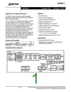
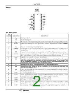
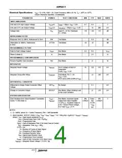
HIP9011
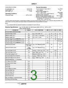
Timing Diagrams
INT/HOLD
CS
t
CIH
t
CSH
t
t
SCCH
t
PWL
CSCH
SCK
t
t
CSCF
PWH
SI
B7 B6 B5
B4
B3
B2
B1
B1
B0
t
SUH
t
HH
SO
B6
B5
B4
B3
B2
B0
B7
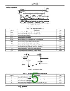
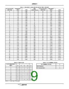
FIGURE 1. SPI TIMING
TABLE 1. SPI TIMING REQUIREMENTS
REQUIREMENT
SYMBOL
TIME
10ns
80ns
60ns
60ns
80ns
20ns
20ns
10ns
10ns
8µs
t
Minimum time from CS falling edge to SCK rising edge.
Minimum time from CS falling edge to SCK falling edge.
Minimum time for the SCK low.
CSCH
t
CSCF
t
PWL
t
Minimum time for the SCK high.
PWH
t
Minimum time from SCK falling after 8 bits to CS raising edge.
Minimum time from data high to falling edge of spiclk.
Minimum time from data low to falling edge of spiclk.
Minimum time for data high after the falling edge of the spiclk.
Minimum time for data low after the falling edge of the spiclk.
Minimum time after CS raises until INT/HOLD goes high.
Minimum time between programming 2 internal registers.
SCCH
t
SUH
t
SUL
t
HH
t
HL
t
CIH
t
200ns
CSH
t3
t1
INT/HOLD
t2
t4
INTOUT
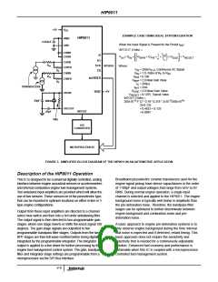
FIGURE 2. INTEGRATOR TIMING
TABLE 2. INTEGRATE/HOLD TIMING REQUIREMENTS
REQUIREMENT
SYMBOL
TIME
45ns
20µs
45ns
20µs
t1
t2
t3
t4
Maximum rise time of the INT/HOLD signal.
Maximum time after INT/HOLD rises for INTOUT to begin to integrate.
Maximum fall time of INT/HOLD signal.
Typical time after INT/HOLD goes low before chip goes into hold state.
4-5

 INTERSIL [ Intersil ]