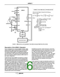
HIP9011
ADDRESS DECODER
PRESCALER/SO TERMINAL STATUS
BANDPASS FILTER
SI
SCK
CS
GAIN CONTROL
SO
INTEGRATOR TIME CONSTANT
TEST/CHANNEL SELECT CONTROL
SI
TEST
COMP OUT
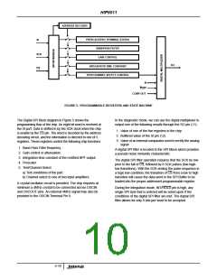
FIGURE 5. PROGRAMMABLE REGISTERS AND STATE MACHINE
The Digital SPI Block diagram in Figure 5 shows the
In the diagnostic mode, we can use the digital multiplexer to
output one of the following results through the SO pin (11):
programming flow of the chip. An eight bit word is received at
the SI port. Data is shifted in by the SCK clock when the chip
is enable by the CS pin. The word is decoded by the address
decoding circuit, and the information is directed to one of 5
registers. These registers control the following chip functions:
1. Value of one of the five registers in the chip
2. Buffered value of the SI pin (12).
3. Value of an internal comparator used to rectify the analog
signal
1. Band Pass Filter frequency.
2. Gain control or attenuation.
3. Integration time constant of the rectified BPF output.
4. Prescaler.
A digital SPI filter is located in the SPI Block which provides
a pseudo noise immunity characteristic.
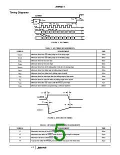
The digital SPI filter operation requires that the SCK be low
prior to the fall of CS, followed by 8 SCK pulses (low-high-
low transitions). With the SCK ending the pulse sequence in
a logic low condition, the transition of CS from a low to high
transition will cause the data-word in the SPI Buffer to be
loaded into the proper addressed programmable register.
5. Test/Channel Select.
a) Test conditions of the part.
b) Channel select to one of two input amplifiers.
A crystal oscillator circuit is provided. The chip requires at
minimum a 4MHz crystal to be connected across OSCIN
and OSCOUT pins. An external 4MHz signal may also be
provided to the OSCIN Terminal Pin 9.
During the Integration mode, INT/HOLD pin is high, any
single SPI byte that is entered will be acted upon if the
conditions of the digital SPI filter are met. The digital SPI
filter allows for only 8 bits per word to be accepted.
4-10

 INTERSIL [ Intersil ]