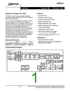
HIP9011
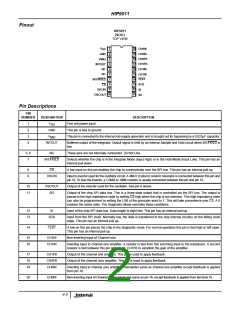
Pinout
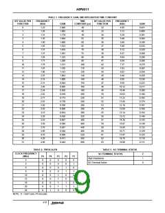
HIP9011
(SOIC)
TOP VIEW
V
1
2
20 CH0NI
DD
GND
19
18
CH0IN
3
CH0FB
VMID
INTOUT
NC
4
17 CH1FB
5
16
15
CH1IN
CH1NI
6
NC
14 TEST
INT/HOLD
CS
7
8
13
12
11
SCK
SI
9
OSCIN
OSCOUT
10
SO
Pin Descriptions
PIN
NUMBER
DESIGNATION
DESCRIPTION
1
2
3
4
V
Five volt power input.
This pin is tied to ground.
DD
GND
V
This pin is connected to the internal mid-supply generator and is brought out for bypassing by a 0.022µF capacitor.
MID
INTOUT
Buffered output of the integrator. Output signal is held by an internal Sample and Hold circuit when INT/HOLD is
low.
5, 6
7
NC
These pins are not internally connected. Do Not Use.
INT/HOLD
Selects whether the chip is in the Integrate Mode (Input High) or in the Hold Mode (Input Low). This pin has an
internal pull down.
8
9
CS
A low input on this pin enables the chip to communicate over the SPI bus. This pin has an internal pull-up.
OSCIN
Input to inverter used for the oscillator circuit. A 4MHz crystal or ceramic resonator is connected between this pin and
pin 10. To bias the inverter, a 1.0MΩ to 10MΩ resistor is usually connected between this pin and pin 10.
10
11
OSCOUT
SO
Output of the inverter used for the oscillator. See pin 9 above.
Output of the chip SPI data bus. This is a three-state output that is controlled via the SPI bus. The output is
placed in the high impedance state by setting CS high when the chip is not selected. This high impedance state
can also be programmed by setting the LSB of the prescaler word to 1. This will take precedence over CS. A 0
enables the active state. The Diagnostic Mode overrides these conditions.
12
13
SI
Input of the chip SPI data bus. Data length is eight bits. This pin has an internal pull-up.
SCK
Input from the SPI clock. Normally low, the data is transferred to the chip internal circuitry on the falling clock
edge. This pin has an internal pull up.
14
TEST
A low on this pin places the chip in the diagnostic mode. For normal operation this pin is tied high or left open.
This pin has an internal pull up.
15
16
CH1NI
CH1IN
Non-inverting input of Channel one.
Inverting input to channel one amplifier. A resistor is tied from this summing input to the transducer. A second
resistor is tied between this pin and pin 17, CH1FB to establish the gain of the amplifier.
17
18
19
CH1FB
CH0FB
CH0IN
Output of the channel one amplifier. This pin is used to apply feedback.
Output of the channel zero amplifier. This pin is used to apply feedback.
Inverting input to channel zero amplifier. Remainder same as channel one amplifier except feedback is applied
from pin 18.
20
CH0NI
Non-inverting input of Channel 0. Remainder the same as pin 16, except feedback is applied from terminal 18.
4-2

 INTERSIL [ Intersil ]