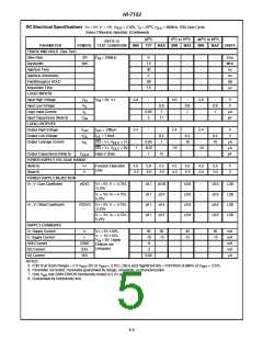
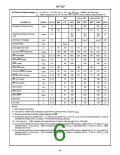
HI-7152
The 5-bit result of the first flash conversion is latched into the
Detailed Description
upper five bits of double buffered latches. It is also converted
back into an analog signal by choosing the ladder voltage
which is closest to but less than the input voltage. The selected
The HI-7152 is a high speed 10-bit A/D converter which
achieves throughput rates of 200kHz by use of a Two Step
Flash algorithm. A pipelined operation has been achieved
through the use of switched capacitor techniques which
allow the device to sample a new input voltage while a
conversion is taking place. The HI-7152 requires a single
reference input of +2.5V, which is internally inverted to -
2.5V, thereby allowing an input range of -2.5V to +2.5V. 10
bits including sign are two’s complement coded. The analog
and reference inputs are internally buffered by high speed
CMOS buffers, which greatly simplifies the external analog
drive requirements for the device.
voltage (V
) is then subtracted from the input voltage. This
TAP
residue is amplified by a factor of 32 and referenced to the neg-
ative reference voltage (V = (V - V ) X 32 + V -).
SCA IN TAP REF
This subtraction and amplification operation is performed by a
Switched Capacitor Amplifier (SCA). The output of the SCA
falls between the positive and negative reference voltages and
can therefore be digitized by the original 5-bit flash converter
(second flash conversion).
The 5-bit result of the second flash conversion is latched into
the lower five bits of double buffered latches. At the end of a
conversion, 10 bits of data plus an Out of Range bit are
latched into the second level of latches and can then be put
on the digital output pins.
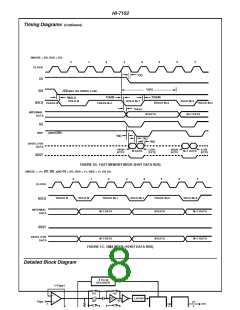
A/D Section
The HI-7152 uses a conversion algorithm which is generally
called a “Two Step Flash” algorithm. This algorithm enables
very fast conversion rates without the penalty of high power
dissipation or high cost. A detailed functional diagram is
presented in Figure 2.
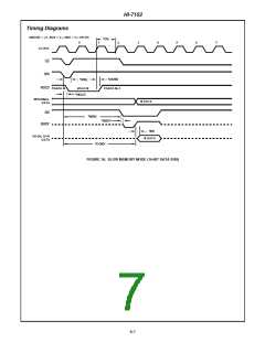
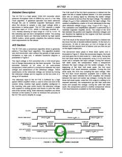
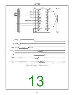
The conversion takes place in three clock cycles and is
illustrated in Figure 3. When the conversion begins, the track
and hold goes into its hold mode for 1 clock cycle. During the
first half clock cycle the comparator array is in its auto-zero
mode and it samples the input voltage. During the second
half clock cycle, the comparators make a comparison
between the input voltage and the ladder voltages. At the
beginning of the third half clock cycle, the first most
significant 5-bit result becomes available. During the first
clock cycle, the SCA was sampling the input voltage. After
the first flash result becomes available and a ladder tap
voltage has been selected the SCA amplifies the residue
between the input and ladder tap voltages. During the next
three half clock cycles, while the SCA output is settling to its
required accuracy, the comparators go into their auto-zero
mode and sample this voltage. During the sixth half clock
cycle, the comparators perform another comparison whose
5-bit result becomes available on the next clock edge.
The input voltage is first converted into a 5-bit result (plus
Out of Range information) by the flash converter. This flash
converter consists of an array of 33 auto-zeroed
comparators which perform a comparison between the input
voltage and subdivisions of the reference voltage. These
subdivisions of the reference voltage are formed by forcing
the reference voltage and its negative on the two ends of a
string of 32 resistors.
The reference input to the HI-7152 is buffered by a high
speed CMOS amplifier which is used to drive one end of the
resistor string. Another high speed amplifier configured in
the inverting unity gain mode inverts the reference voltage
with respect to analog ground and forces in onto the other
end of the resistor string. Both reference amplifiers are offset
trimmed at the factory in order to increase the accuracy of
the HI-7152 and to simplify its usage.
N CONVERSION
N + 1 CONVERSION
CLOCK
1
2
3
4
5
6
TRACK AND HOLD
HOLD V (N)
IN
TRACK V (N + 1)
IN
HOLD V (N + 1)
IN
CONVERT
UPPER
5 BITS
CONVERT
LOWER
5 BITS
COMPARATOR
AUTO-ZERO
(AZ)
SAMPLE
(N)
SAMPLE RESIDUAL
SAMPLE
V
V (N + 1)
IN
IN
SCA AUTO-ZERO
(SCAZ)
SAMPLE V (N)
IN
AMPLIFY RESIDUAL
SAMPLE V (N + 1)
IN
INTERNAL DATA
10-BITS + OVR
V
(N) DATA
IN
FIGURE 3. INTERNAL ADC TIMING DIAGRAM
6-9

 INTERSIL [ Intersil ]