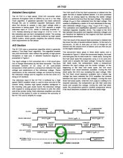
HI-7152
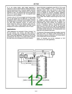
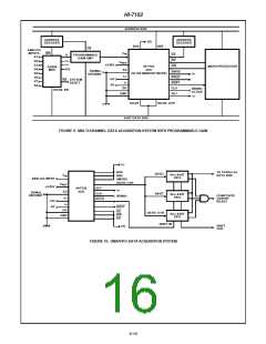
As in any analog system, good supply bypassing is Figure 8 illustrates an application where the HI-7152 is used
necessary in order to achieve optimum system performance with an analog multiplexer to form a multi-channel data
(minimize conversion errors). The power supplies should be acquisition system. Either slow memory or fast memory
bypassed with at least a 20µF tantalum and 0.1µF ceramic modes of operation can be selected. Fast memory mode
capacitors to GND. The reference input should be bypassed should be selected for maximum throughput. Multiplexer
with a 0.1µF ceramic capacitor to AG. The capacitor leads channel acquisition should occur approximately 500ns after
should be as short as possible.
HOLD goes high. This allows 2 clocks minus 0.5µs for the
input to settle. With a 600kHz clock the input has up to 2.8µs
to settle.
The pins on the HI-7152 are arranged such that the analog
pins are well isolated from the digital pins. In spite of this
arrangement, there is always pin to pin coupling. Therefore An intelligent system which performs
a scale factor
the analog inputs to the device should not be driven from adjustment under software control with the addition of a
very high output impedance sources. PC board layout programmable gain block between the multiplexer and
should screen the analog and reference inputs with AG. HI-7151 is illustrated in Figure 9. The microprocessor first
Using a soldier mask is good practice and helps reduce performs a conversion and then checks the over-range
leakage due to moisture contamination on the PC board.
status (OVR) bit. If the OVR bit is high, the microprocessor
addresses a precision gain circuit for scale factor adjustment
and initiates another conversion. The microprocessor must
keep track of the selected scale factor.
Applications
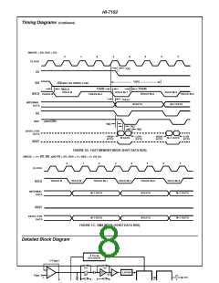
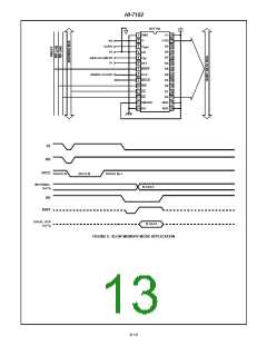
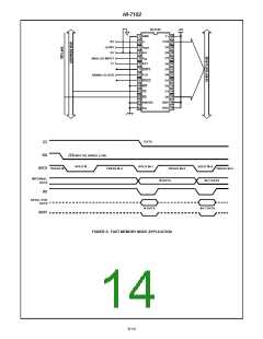
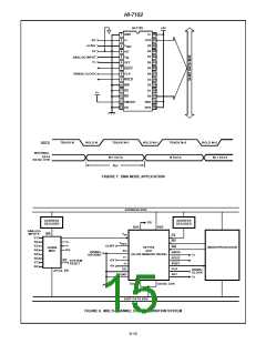
Typical applications are illustrated in Figure 5 through 7 for
the slow memory, fast memory, and DMA modes of
operation. The output data is configured for 16-bit bus oper-
ation of these three applications. By tying BUS and DG and
connecting the HBE input to the system address decoder,
the output data can be configured for 8-bit bus systems.
The accuracy of the programmable gain amplifier should be
better than 0.05%. For optimum system performance, op
amp frequency response, settling time, and charge injection
of the analog switch must be considered.
Figure 10 illustrates the HI-7152 interfaced to FIFO
memories for use in DMA applications.
20µF
-
0.1µF
5V
P.S.
+
+
+
HI-7152
2.5V
P.S.
-5V
P.S.
1 GND
2 V-
V+ 28
OVR 27
D9 26
0.1µF
20µF
-
-
3
V
REF
4 AG
5 V
0.1µF
D8 25
ANALOG INPUT
V+
D7 24
IN
6 SET
7 BUSY
8 CLK
D6 23
D5
22
D4 21
20
9 HOLD
10 WR
D3
D2 19
D1 18
11 CS
D0 17
12 RD
13 SMODE
14 DG
HBE 16
BUS 15
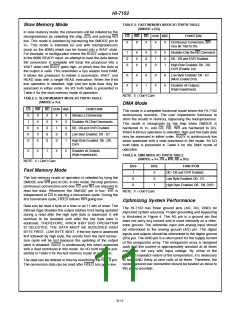
FIGURE 4. GROUND AND POWER SUPPLY DECOUPLING
6-12

 INTERSIL [ Intersil ]