HI-7152
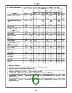
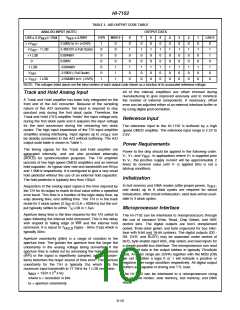
TABLE 1. A/D OUTPUT CODE TABLE
ANALOG INPUT (NOTE)
) / 1024 = 2.500V
OUTPUT DATA
LSB = 2 (V
V
OVR
MSB 9
8
0
1
0
0
1
0
0
7
0
1
0
0
1
0
0
6
0
1
0
0
1
0
0
5
0
1
0
0
1
0
0
4
0
1
0
0
1
0
0
3
0
1
0
0
1
0
0
2
0
1
0
0
1
0
0
1
0
1
0
0
1
0
0
LSB 0
REF
REF
≥ +V
2.500V to V+ (+OVR)
2.49512V (+Full Scale)
0.00488V
1
0
0
0
0
0
1
0
0
0
0
1
1
1
0
1
1
0
1
0
0
REF
+V
- 1 LSB
REF
+1 LSB
0
0.000V
-1 LSB
-0.00488V
-V
-2.500V (-Full Scale)
-2.50488V to V- (-OVR)
REF
REF
≤ -V
- 1 LSB
NOTE: The voltages listed above are the ideal centers of each output code shown as a function of its associated reference voltage.
All of the internal amplifiers are offset trimmed during
manufacturing to give improved accuracy and to minimize
Track and Hold Analog Input
A Track and Hold amplifier has been fully integrated on the
front end of the A/D converter. Because of the sampling
nature of this A/D converter, the input is required to stay
constant only during the first clock cycle. Therefore, the
Track and Hold (T/H) amplifier “holds” the input voltage only
during the first clock cycle and it acquires the input voltage
for the next conversion during the remaining two clock
cycles. The high input impedance of the T/H input amplifier
the number of external components. If necessary, offset
error can be adjusted either at an external interface buffer or
by using digital post correction.
Reference Input
The reference input to the HI-7152 is buffered by a high
speed CMOS amplifier. The reference input range is 2.2V to
2.6V.
simplifies analog interfacing. Input signals up to ±V
can
REF
be directly connected to the A/D without buffering. The A/D
output code table is shown in Table 1.
Power Requirements
The timing signals for the Track and Hold amplifier are
generated internally, and are also provided externally
(HOLD) for synchronization purposes. The T/H amplifier
consists of two high speed CMOS amplifiers and an internal
hold capacitor. Its typical slew rate and bandwidth are 9V/µs
and 1.5MHz respectively. It is configured to give a very small
hold pedestal without the use of an external hold capacitor.
The hold pedestal is typically less than 100µV.
Power to the chip should be applied in the following order:
V-, V+, and V
. In applications where V+ is supplied prior
REF
to V-, the positive supply current will be approximately 2
times its nominal value until V- is applied (this is not a
latchup condition).
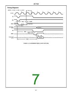
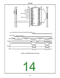
Initialization
In fast memory and DMA modes (after proper power, V
,
Acquisition of the analog input signal is the time required by
the T/H for its output to reach its final value within a specified
error band. This time is a function of the logic delay time, op
amp slewing time, and settling time. The T/H is in the track
REF
and clock) up to 6 clock cycles are required for circuit
initialization. After circuit initialization, valid data will be avail-
able in 3 clock cycles.
mode for 2 clock cycles (3.3µs at CLK = 600kHz) but the out-
1
put typically settles to within / LSB in 1.5µs.
Microprocessor Interface
4
Aperture delay time is the time required for the T/H switch to
open following the internal hold command. This is the delay
with respect to falling edge of WR and the internal hold
The HI-7152 can be interfaced to microprocessors through
the use of standard Write, Read, Chip Select, and HBE
control pins. The digital outputs are two’s complement
coded, three-state gated, and byte organized for bus inter-
face with 8-bit and 16-bit systems. The digital outputs (D0 -
D9, OVR, and BUSY) may be accessed under control of
BUS, byte enable input HBE, chip select, and read inputs for
a simple parallel bus interface. The microprocessor can read
the current data in the output latches in typically 75ns/byte
(trd). An over range pin (OVR) together with the MSB (D9)
pin set to either a logic 0 or 1 will indicate a positive or
negative over-range condition respectively. All digital output
buffers are capable of driving one TTL load.
command. It is equal to T
typically 30ns.
(type) - 50ns (Typ) which is
HOLD
Aperture uncertainty (jitter) is a range of variation in the
aperture time. The greater the aperture time the larger the
uncertainty in the analog voltage being converted. If the
aperture time is nulled out by advancing the hold command
(WR) or the signal is repetitively sampled, aperture uncer-
tainty becomes the major source of time error. The aperture
uncertainty for the T/H is typically 2ns which sets the
maximum input bandwidth to 77.7kHz for 1 LSB resolution.
n
f
= 1/(2π x 2 x ta)
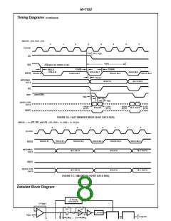
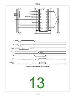
The HI-7152 can be interfaced to a microprocessor using
one of three modes: slow memory, fast memory, and DMA
mode.
MAX
where n = resolution in bits
ta = aperture uncertainty
6-10

 INTERSIL [ Intersil ]