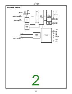
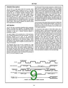
HI-7152
o
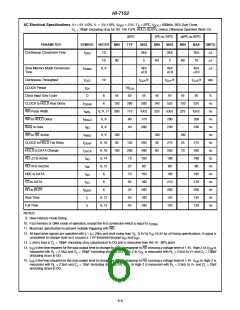
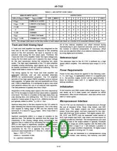
AC Electrical Specifications V+ = 5V ±10%, V- = -5V ±10%, V
= 2.5V, T = 25 C, f
= 600kHz, 50% Duty Cycle,
REF
A
CLK
C
= 100pF (including stray for D0 - D9, OVR, HOLD, BUSY), Unless Otherwise Specified (Note 12)
L
o
o
o
o
o
25 C
0 C to 75 C
-40 C to 85 C
PARAMETER
SYMBOL NOTES MIN
TYP
MAX
3tck
5
MIN
MAX
3tck
5
MIN
MAX
3tck
10
UNITS
µs
Continuous Conversion Time
t
10
10
-
60
-
-
-
-
-
60
-
-
60
-
SPS
µs
Slow Memory Mode Conversion
Time
t
CONV
6, 9
4tck
+0.9
4tck
+0.9
4tck
+0.9
µs
Continuous Throughput
CLOCK Period
t
10
-
-
-
f
/3
-
f
/3
-
f
/3
sps
CYC
CLK
CLK
CLK
-
t
-
1/f
-
-
-
-
CK
CLK
Clock Input Duty Cycle
CLOCK to HOLD Rise Delay
WR Pulse Width
WR to HOLD Delay
Busy to Data
D
6
45
50
55
500
tck/2
170
200
-
45
55
525
tck/2
200
230
-
45
55
525
tck/2
200
230
-
%
t
CKHR
6
150
290
113
80
40
-
140
120
ns
ns
ns
ns
ns
ns
ns
ns
ns
ns
ns
ns
ns
ns
t
6, 9, 11
6, 9
6, 9
6, 9
6, 10
6, 10
6, 14
6, 15
6
200
225
225
WRL
t
-
-
-
HOLD
t
-
-
-
BD
WR to RD Active
CLOCK to HOLD Fall Delay
HOLD to DATA Change
RD LO to Active
RD HI to Inactive
HBE to DATA
t
100
100
100
WRD
CKHF
DATA
t
t
50
125
200
75
25
70
95
35
50
45
250
400
150
60
40
90
-
275
550
190
80
25
70
-
275
550
190
80
100
t
-
-
-
-
-
-
-
RD
t
-
-
RX
AD
CD
t
150
180
200
100
100
-
165
210
200
125
120
-
165
210
200
125
120
CS to DATA
t
6
-
-
RD to BUSY
t
6
-
-
BUSY
Rise Time
t
6, 13
6, 13
-
-
r
f
Fall Time
t
-
-
NOTES:
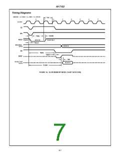
9. Slow memory mode timing.
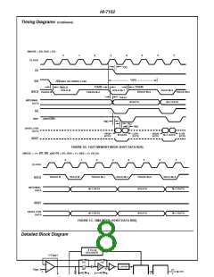
10. Fast memory or DMA mode of operation, except the first conversion which is equal to t
11. Maximum specification to prevent multiple triggering with WR.
.
CONV
12. All input drive signals are specified with t = t ≤ 20ns and shall swing from V -0.4V to V +0.4V for all timing specifications. A signal is
IL IH
r
f
considered to change state as it crosses a 1.4V threshold (except t
and t ).
RD
RX
13. t and t load is C = 100pF (including stray capacitance) to DG and is measured from the 10 - 90% point.
r
f
L
14. t
is the time required for the data output level to change by 10% in response to RD crossing a voltage level of 1.4V. High-Z to V
is
RD
OH
is measured with R = 2.5kΩ to V+ and C = 100pF
measured with R = 2.5kΩ and C = 100pF (including stray) to DG. High-Z to V
L
L
OL
L
L
(including stray) to DG.
15. t
is the time required for the data output level to change by 10% in response to RD crossing a voltage level of 1.4V. V
to High-Z is
RX
OH
to High-Z is measured with R = 2.5kΩ to V+ and C = 10pF
measured with R = 2.5kΩ and C = 10pF (including stray) to DG. V
L
L
OL
L
L
(including stray) to DG.
6-6

 INTERSIL [ Intersil ]