HI-7152
TABLE 3. FAST MEMORY MODE I/O TRUTH TABLE
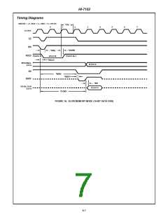
Slow Memory Mode
(SMODE = DG)
In slow memory mode, the conversion will be initiated by the
microprocessor by selecting the chip (CS) and pulsing WR
low. This mode is selected by hardwiring the SMODE pin to
V+. This mode is intended for use with microprocessors
(such as the 8086) which can be forced into a WAIT state.
For example, in configuration where the BUSY output is tied
to the 8086 READY input, an attempt to read the data before
the conversion is complete will force the processor into a
WAIT state until BUSY goes high, at which time the data at
the output is valid. This resembles a 5µs access time RAM.
It allows the processor to initiate a conversion, WAIT, and
READ data with a single READ instruction. When the 8-bit
bus operation is selected, high and low byte data may be
accessed in either order. An I/O truth table is presented in
Table 2 for the slow memory mode of operation.
CS WR RD BUS HBE
FUNCTION
X
0
X
X
X
Continuous Conversion, WR
may be Tied to DG.
1
0
0
X
X
X
X
0
0
X
1
0
X
X
1
Disables Only the RD Command.
D0 - D9 and OVR Enabled.
High Byte Enabled: D8 - D9,
OVR (Enable 1st).
0
X
X
0
1
0
0
Low Byte Enabled: D0 - D7
(Must Enable 2nd).
X
X
X
Disables All Outputs
(High Impedance).
NOTE: X = Don’t Care
TABLE 2. SLOW MEMORY MODE I/O TRUTH TABLE
(SMODE = V+)
DMA Mode
CS WR RD BUS HBE
FUNCTION
This mode is a complete hardware mode where the HI-7152
continuously converts. The user implements hardware to
store the results in memory, bypassing the microprocessor.
This mode is recognized by the chip when SMODE is
hardwired to V+ and CS, RD, WR are hardwired to DG.
When 8-bit bus operation is selected, high and low byte data
may be accessed in either order. BUSY is continuously low
when accessed with a read command in this mode. An I/O
truth table is presented in Table 4 for the DMA mode of
operation.
0
1
0
0
0
0
X
X
X
X
X
X
0
0
0
X
X
1
0
0
X
X
X
0
Initiates a Conversion.
Disables All Chip Commands.
D0 - D9 and OVR Enabled.
Low Byte Enabled: D0 - D7.
1
High Byte Enabled: D8 - D9,
OVR.
X
X
1
X
X
Disables all Outputs
(High Impedance).
TABLE 4. DMA MODE I/O TRUTH TABLE
(SMODE = V+, CS = WR, RD = DG)
NOTE: X = Don’t Care
BUS
HBE
FUNCTION
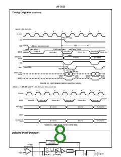
Fast Memory Mode
1
0
0
X
0
1
D0 - D9 and OVR Enabled.
Low Byte Enabled: D0 - D7.
High Byte Enabled: D8 - D9, OVR.
The fast memory mode of operation is selected by tying the
SMODE and WR pins to DG. In this mode, the chip performs
continuous conversions and only CS and RD are required to
read the data. Whenever the SMODE pin is low, WR is
independent of CS in starting a conversion cycle. During the
first conversion cycle, HOLD follows WR going low.
NOTE: X = Don’t Care
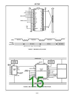
Optimizing System Performance
Data can be read a byte at a time or all 11 bits at once. The
internal logic disables the output latches from being updated
during a read after the high byte data is accessed. It will
continue to be disabled until after the low byte data is
accessed. THEREFORE, WHEN 8-BIT BUS OPERATION
IS SELECTED, THE DATA MUST BE ACCESSED HIGH
BYTE FIRST, LOW BYTE NEXT. If the low byte is accessed
first followed by high byte, the results from the next conver-
sion cycle will be lost because the updating of the output
latch is disabled. BUSY is continuously low when accessed
with a read command in this mode. An I/O truth table is pre-
sented in Table 3 for the fast memory mode of operation.
The HI-7152 has three ground pins (AG, DG, GND) for
improved system accuracy. Proper grounding and bypassing
is illustrated in Figure 4. The AG pin is a ground pin that
does not carry any current and is used internally as a refer-
ence ground. The reference input and analog input should
be referenced to the analog ground (AG) pin. The digital
inputs and outputs should be referenced to the digital ground
(DG) pin. The GND pin is a return point for the supply current
of the comparator array. The comparator array is designed
such that this current is approximately constant at all times
and does not vary with input voltage. By virtue of the
switched capacitor nature of the comparators, it is necessary
to hold GND firmly at zero volts at all times. Therefore, the
system ground star connection should be located as close to
this pin as possible.
The data can be defined in time by monitoring the HOLD pin.
The conversion data can be read after HOLD has gone low.
6-11

 INTERSIL [ Intersil ]