HI-7152
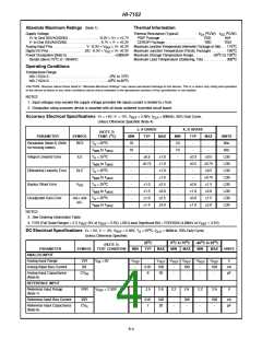
Absolute Maximum Ratings (Note 1)
Supply Voltage
Thermal Information
Thermal Resistance (Typical)
o
o
θ
( C/W)
θ
( C/W)
JA
JC
V+ to Gnd (DG/AG/GND) . . . . . . . . . . . . . . . . -0.3V < V+ < +5.7V
V- to Gnd (DG/AG/GND). . . . . . . . . . . . . . . . . .-5.7V < V- < +0.3V
PDIP Package . . . . . . . . . . . . . . . . . . .
CERDIP Package . . . . . . . . . . . . . . . .
Maximum Junction Temperature (Hermetic Package or Die). . . 175 C
Maximum Junction Temperature (Plastic Package) . . . . . . . . 150 C
Maximum Storage Temperature Range . . . . . . . . . .-65 C to 150 C
TBD
TBD
N/A
TBD
o
o
o
o
Analog Input Pins . . . . . . . . . . . . . . . . . V- -0.3V < V
< V+ +0.3V
INA
Digital I/O Pins . . . . . . . . . . . . . . . . . . .DG - 0.3V < V < V+ +0.3V
I/O
o
Power Dissipation (Note 2). . . . . . . . . . . . . . . . . . . . . . . . . <500mW
o
Derate above 75 C at -10mW/C
Maximum Lead Temperature (Soldering, 10s) . . . . . . . . . . . . 300 C
Operating Conditions
Temperature Range
HI3-7152X-5 . . . . . . . . . . . . . . . . . . . . . . . . . . . . . . . .0 C to 75 C
HI3-7152X-9 . . . . . . . . . . . . . . . . . . . . . . . . . . . . . . -40 C to 85 C
o
o
o
o
CAUTION: Stresses above those listed in “Absolute Maximum Ratings” may cause permanent damage to the device. This is a stress only rating and operation
of the device at these or any other conditions above those indicated in the operational sections of this specification is not implied.
NOTES:
1. Input voltages may exceed the supply voltage provided the inputs current is limited to ±1mA.
2. Dissipation rating assumes device is mounted with all leads soldered to printed circuit board.
Accuracy Electrical Specifications V+ = +5V, V- = -5V, V
= 2.50V, f
CLK
= 600kHz, 50% Duty Cycle,
REF
Unless Otherwise Specified (Note 4)
J, A GRADE
K, B GRADE
(NOTE 3)
TEMP. ( C)
o
PARAMETER
SYMBOL
MIN
TYP
-
MAX
-
MIN
TYP
-
MAX
-
UNITS
Bits
o
Resolution (Note 5) (With
no missing codes)
RES
T
T
T
T
T
T
T
T
T
T
= 25 C
10
10
-
10
10
-
A
to T
o
-
-
-
-
Bits
MIN
MAX
Integral Linearity Error
Differential Linearity Error
Bipolar Offset Error
Unadjusted Gain Error
NOTES:
ILE
= 25 C
±0.5
±0.75
-
±1.0
±1.0
±1.0
±1.0
±2.5
±3.0
±2.5
±3.0
±0.3
±0.5
-
±0.5
±0.75
±0.5
±0.75
±1.5
±2.0
±1.5
±2.0
LSB
LSB
LSB
LSB
LSB
LSB
LSB
LSB
A
to T
o
-
-
MIN
MAX
DLE
= 25 C
-
-
A
to T
o
-
-
-
-
MIN
MAX
V
= 25 C
-
±1.0
±1.5
±1.0
±1.5
-
±0.6
±1.0
±0.6
±1.0
OS
A
to T
o
-
-
MIN
MAX
eG+ and
eG-
= 25 C
-
-
A
to T
-
-
MIN
MAX
3. See Ordering Information Table.
4. FSR (Full Scale Range) = 2 X V
(5V at V
= 2.5V). LSB (Least Significant Bit) = FSR/1024 (4.88mV at V
o
= 2.5V).
REF
REF
REF
DC Electrical Specifications V+ = 5V, V- = -5V, V
= 2.50V, T = 25 C, f
= 600kHz, 50% Duty Cycle,
CLK
REF
A
Unless Otherwise Specified
o
o
o
o
o
25 C
0 C to 75 C
MIN MAX
-40 C to 85 C
MIN MAX
(NOTE 5)
TEST CONDITION
PARAMETER
ANALOG INPUT
SYMBOL
MIN
TYP
MAX
UNITS
Analog Input Range
VIR
IBI
V
= 0V
-V
REF
-
0.01
8
V
-V
REF
V
-V
REF
V
REF
V
IN
REF
REF
Analog INput Bias Current
-
-
100
20
-
-
100
-
-
-
100
-
nA
pF
Analog Input Capacitance
(Note 6)
CV
IN
REFERENCE INPUT
Reference Input Range
(Note 7)
VRR
IBR
V
= 2.50V
2.2
2.5
2.6
2.2
2.6
2.2
2.6
V
REF
Reference Input Bias Current
-
-
0.01
7
100
20
-
-
100
-
-
-
100
-
nA
pF
Reference Input Capacitance
(Note 6)
CV
R
6-4

 INTERSIL [ Intersil ]