HI-7152
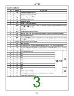
Pin Descriptions
PIN
SYMBOL
DESCRIPTION
1
GND
Ground return for comparators (0V).
2
V-
Negative supply voltage input (-5V).
Reference voltage input (+2.50V).
Analog ground reference (0V).
Analog Input Voltage.
3
V
REF
4
AG
5
V
IN
6
SET
Connect to V+ for proper operation.
7
BUSY
Output High-Conversion complete. Output Low - Conversion in progress. Output floats when chip is not se-
lected (RD and CS both high).
8
CLK
HOLD
WR
Clock input.
9
Indicates start of conversion. Active low.
10
11
12
Write input. With CS low, starts conversion when pulsed low; continuous conversions when kept low.
Chip select input. Active low.
CS
RD
Read input. With CS low, enables output buffers when pulsed low; outputs updated at end of conversion
when kept low.
13
14
15
16
SMODE
DG
Slow memory mode input. Active high.
Digital ground (0V).
BUS
Bus select input. High = all outputs enabled together D0 - D9, OVR. Low = outputs enabled by HBE.
HBE
Byte select (HBE/LBE) input for 8-bit bus. Input high-High byte select, D8-D9, OVR Input low-low byte select,
D0-D7.
17
18
19
20
21
22
23
24
25
26
27
28
D0
D1
D2
D3
D4
D5
D6
D7
D8
D9
OVR
V+
Bit 0 (Least significant, LSB).
Bit 1.
Bit 2.
Bit 3.
Low
Byte
Bit 4.
Output Data Bits
(High = True)
Bit 5.
Bit 6.
Bit 7.
Bit 8.
High
Byte
Bit 9 (Most Significant, MSB).
Out of Range flag. Valid at end of conversion when output exceeds full scale.
Positive supply voltage input (+5V).
6-3

 INTERSIL [ Intersil ]