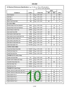
HS-3282
• The Line Receiver functions as a voltage level translator.
It transforms the 10 volt differential line voltage, ARINC
429 format, into 5 volt internal logic level.
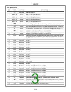
TABLE 2B. WORD 2 FORMAT
BI-DIRECTIONAL
BlT#
FUNCTION
ARINC BIT#
• The output of the Line Receiver is one of two inputs to the
Self-Test Data Selector (SEL). The other input to the
Data Selector is the Self-Test Signal from the Transmitter
section.
15
Sign
29
28
14
MSB
13 - 00
Data
27 - 14
• The incoming data, either Self-Test or ARlNC 429, is
double sampled by the Word Gap Timer to generate a
Data Clock. The Receiver sample frequency (RCVCLK),
1MHz, or 125kHz, is generated by the Receiver/Transmit-
ter Timing Circuit. This sampling frequency is ten times the
Data Rate to ensure no data ambiguity.
Receiver Parity Status:
0 = Odd Parity
1 = Even Parity
If the receiver input data word string is broken before the
entire data word is received, the receiver will reset and
ignore the partially received data word.
• The derived data clock then shifts the data down a 32-Bit
long Data Shift Register (Data S/RI). The Data Word
Length is selectable for either 25 Bits or 32 Bits long by the
Control Signal (WLSEL). As soon as the data word is
completely received, an internal signal (WDCNT1) is gen-
erated by the Word Gap Timer Circuit.
If the transmitter is used to transmit consecutive data words,
each word will be separated by a four (4) bit “null” state (both
positive and negative outputs will maintain a zero (0) volt
level.)
• The Source/Destination (S/D) Decoder compares the user
set code (X and Y) with Bits 9 and 10 of the Data Word. If
the two codes are matched, a positive signal is generated
to enable the WDCNT1 signal to latch in the received data.
Otherwise, the data word is ignored and no latching action
takes place. The S/D Decoder can be Enabled and
Disabled by the control signal S/D ENB. If the data word is
latched, an indicator flag (D/R1) is set. This indicates a
valid data word is ready to be fetched by the user.
TABLE 3. ARINC 25-BIT DATA FORMAT
ARINC BIT #
FUNCTION
Label
1 - 8
9
LSB
11 - 23
24
Data
MSB
25
Parity Status
• After the receiver data has been shifted down the shift
register, it is placed in a holding register. The device ready
flag will then be set indicating that data is ready to be
fetched. If the data is ignored and left in the holding regis-
ter, it will be written over when the next data word is
received.
TABLE 4A. WORD 1 FORMAT
BI-DIRECTIONAL
BIT#
FUNCTION
Don’t Care
Parity Status
Label
ARINC BIT#
15 - 9
8
XXX
25
• The received data in the 32-bit holding register is placed
on the bus in the form of two (2)16-bit words regardless of
whether the format is for 32 or 25-bit data words. Either
word can be accessed first or repeatedly until the next
received data word falls into the holding register.
7 - 0
1 - 8
TABLE 4B. WORD 2 FORMAT
BI-DIRECTIONAL
• The parity of the incoming word is checked and the status
(i.e., logic “0” for odd parity and logic “1” for even parity)
stored in the receiver latch and output on BD08 during the
Word No. 1.
BIT#
FUNCTION
ARINC BlT#
15
MSB
24
23 -10
9
14 - 1
0
Data
LSB
• Assuming the user desires to access the data, he first sets
the Data Select Line (SEL) to a Logic “0” level and pulses
the Enable (EN1) line. This action causes the Data
Selector (SELl) to select the first-data word, which con-
tains the label field and Enable it onto the Data Bus. To
obtain the second data word, the user sets the SEL line to
a Logic “1” level and pulse the Enable (EN1) line again.
The Enable pulse duration is matched to the user circuit
requirement needed to read the Data Word from the Data
Bus. The second Enable pulse is also used to reset the
Device Ready (D/R1) flip-flop. This completes a receiving
cycle.
Receiver Parity Status:
0 = Odd Parity
1 = Even Parity
No Source/Destination (S/D) in 25-Bit format.
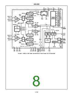
Receiver Operation
Since the two receivers are functionally identical, only one
will be discussed in detail, and the block diagram will be
used for reference in this discussion. The receiver consists
of the following circuits:
5-188

 INTERSIL [ Intersil ]