HS-3282
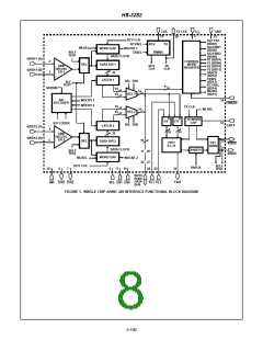
Operational Description
The HS-3282 is designed to support ARINC Specification Provisions have been made through the external clock input
429 and other serial data protocols that use a similar format to provide data rate flexibility. This requires an external clock
by collecting the receiving, transmitting, synchronizing, that is 10 times the data rate.
timing and parity functions on a single, low power LSl circuit.
To obtain the flexibility discussed above, a number of
It goes beyond the ARlNC requirements by providing for
external control signals are required, To reduce the pin count
either odd or even parity, and giving the user a choice of
requirements, an internal control word register is used. The
either 25 or 32-bit word lengths. The receiver and transmitter
control word is latched from the data bus into the register by
sections operate independently of each other. The serial-to-
the Control Word Strobe (CWSTR) signal going to a logic
parallel conversion required of the receiver and the parallel-
“1”. Eleven (11) control functions are used, and along with
to-serial conversion requirements of the transmitter have
the Bus Data (BD) line are listed below:
been incorporated into the bus interface circuit.
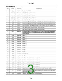
Control Word
PIN NAME SYMBOL
FUNCTION
BD05
SLFTST
Connects the self test signal from the transmitter directly to the receiver shift registers, bypassing the input
receivers. Receiver 1 receives Data True and Receiver 2 receives Data Not. Note that the transmitter output
remains active. (Logic “0” on SLFTST Enables Self Test).
BD06
BD07
SDENB1 Signal to Activate the Source/Destination (S/D) Decoder for Receiver 1. (Logic “1” activates S/D Decoder).
X1
If SDENB1 = “1” then this bit is compared with ARlNC Data Bit #9. If Y1 also matches (see Y1), the word will be
accepted by the Receiver 1. If SDENB1 = “0” this bit becomes a don’t care.
BD08
Y1
If SDENBI = “1” then this bit is compared with ARINC Data Bit #10. If X1 also matches (see X1), the word will
be accepted by the Receiver 1. If SDENB1 = “0” this bit becomes a don’t care.
BD09
BD10
SDENB2 Signal to activate the Source/Destination (S/D) Decoder for Receiver 2. (Logic “1” activates S/D Decoder).
X2
If SDENB2 = “1” then this bit is compared with ARlNC Data Bit #9. If Y2 also matches (see Y2), the word will be
accepted by the Receiver 2. If SDENB2 = “0” this bit becomes a don’t care.
BD11
BD12
BD13
BD14
Y2
If SDENB2 = “1” then this bit is compared with ARINC Data Bit #10. If X2 also matches (see X2), the word will
be accepted by the Receiver 2. If SDENB2 = “0” this bit becomes a don’t care.
PARCK
TXSEL
Signal used to invert the transmitter parity bit for test of parity circuits. Logic “0” selects normal odd parity. Logic
“I” selects even parity.
Selects high or low Transmitter data rate. If TXSEL = “0” then transmitter data rate is equal to the clock rate
divided by ten (10). If TXSEL = “1” then transmitter data rate is equal to the clock rate divided by eighty (80).
RCVSEL Selects high or low Receiver data rate. If RCVSEL = “0” then the received data rate should be equal to the clock
rate divided by ten (10), if RCVSEL = “1 “then the received data rate should be equal to the clock rate divided
by eighty (80).
BD15
WLSEL
Selects word length. If WLSEL = “0” a 32-bit word format will be selected. If WLSEL = “1” a 25-Bit word format
will be selected.
ARlNC 429 DATA FORMAT as input to the Receiver and out- This format is shuffled when seen on the sixteen bidirec-
put from the Transmitter is as follows:
tional input/outputs. The format shown below is used from
the receivers and input to the transmitter:
TABLE 1. ARINC 429 32-BIT DATA FORMAT
TABLE 2A. WORD 1 FORMAT
ARINC BIT #
1 - 8
FUNCTION
Label
BI-DIRECTIONAL
BIT #
15, 14
13
FUNCTION
Data
ARINC BlT #
13, 12
11
9 - 10
11
SDl or Data
LSB
LSB
12 - 27
28
Data
12, 11
10, 9
8
SDl or Data
SSM Status
Parity Status
Label
10, 9
MSB
31, 30
32
29
Sign
30, 31
32
SSM
7 - 00
1 - 8
Parity Status
5-187

 INTERSIL [ Intersil ]