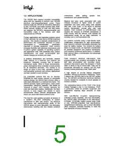
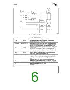
28F020
E
DQ0 - DQ7
VCC
VSS
VPP
Erase Voltage
Switch
Input/Output
Buffers
To Array Source
State
Control
WE#
Command
Register
Integrated Stop
Timer
PGM Voltage
Switch
Chip Enable
Output Enable
Logic
STB
Data Latch
Y-Gating
CE#
OE#
Y-Decoder
X-Decoder
STB
A0 - A17
2,097,152 Bit
Cell Matrix
0245_01
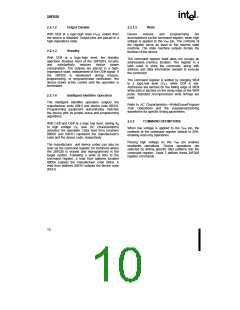
Figure 1. 28F020 Block Diagram
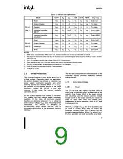
Table 1. Pin Description
Symbol
Type
INPUT
Name and Function
A0–A17
ADDRESS INPUTS for memory addresses. Addresses are
internally latched during a write cycle.
DQ0–DQ7
INPUT/OUTPUT
DATA INPUT/OUTPUT: Inputs data during memory write cycles;
outputs data during memory read cycles. The data pins are active
high and float to tri-state off when the chip is deselected or the
outputs are disabled. Data is internally latched during a write cycle.
CE#
INPUT
CHIP ENABLE: Activates the device’s control logic, input buffers,
decoders and sense amplifiers. CE# is active low; CE# high
deselects the memory device and reduces power consumption to
standby levels.
OE#
WE#
INPUT
INPUT
OUTPUT ENABLE: Gates the devices output through the data
buffers during a read cycle. OE# is active low.
WRITE ENABLE: Controls writes to the control register and the
array. Write enable is active low. Addresses are latched on the
falling edge and data is latched on the rising edge of the WE#
pulse.
Note: With VPP ≤ 6.5 V, memory contents cannot be altered.
VPP
ERASE/PROGRAM POWER SUPPLY for writing the command
register, erasing the entire array, or programming bytes in the array.
VCC
VSS
DEVICE POWER SUPPLY (5 V ±10%)
GROUND
6

 INTEL [ INTEL ]