Electrical Specifications
Figure 4. Deeper Sleep VCC and ICC Processor Loadline
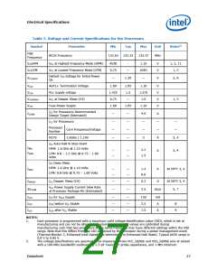
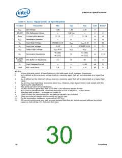
Table 8. FSB Differential BCLK Specifications
Symbol
Parameter
Min
Typ
Max
Unit
Figure
Notes1
VIH
Input High Voltage
—
—
1.15
V
7, 8
VOH
VCROSS
ΔVCROSS
VSWING
ILI
Input Low Voltage
—
0.3
—
—
—
-0.3
0.55
140
—
V
V
7, 8
Crossing Voltage
2, 7, 9
Range of Crossing Points
Differential Output Swing
Input Leakage Current
Pad Capacitance
—
mV
mV
µA
pF
2, 7, 5
300
-5
—
6
3
4
—
+5
Cpad
1.2
1.45
2.0
NOTES:
1.
2.
Unless otherwise noted, all specifications in this table apply to all processor frequencies.
Crossing Voltage is defined as absolute voltage where rising edge of BCLK0 is equal to the falling edge of
BCLK1.
3.
4.
5.
6.
7.
8.
9.
For Vin between 0 V and VIH.
Cpad includes die capacitance only. No package parasitics are included.
ΔVCROSS is defined as the total variation of all crossing voltages as defined in note 2.
Measurement taken from differential waveform.
Measurement taken from single-ended waveform.
“Steady state” voltage, not including Overshoots or Undershoots.
Only applies to the differential rising edge (BCLK0 rising and BCLK1 falling).
Datasheet
29

 INTEL [ INTEL ]