Electrical Specifications
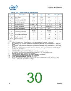
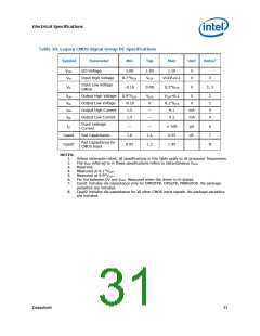
Table 10. Legacy CMOS Signal Group DC Specifications
Symbol
Parameter
I/O Voltage
Min
Typ
Max
Unit
Notes1
VCCP
VIH
1.00
1.05
VCCP
1.10
V
V
Input High Voltage
0.7*VCCP
VCCP+0.1
2
Input Low Voltage
CMOS
VIL
-0.10
0.00
0.3*VCCP
V
2, 3
VOH
VOL
IOH
IOL
Output High Voltage
Output Low Voltage
Output High Current
Output Low Current
0.9*VCCP
-0.10
1.5
VCCP
0
VCCP+0.1
0.1*VCCP
4.1
V
2
2
5
4
V
—
mA
mA
1.5
—
4.1
Input Leakage
Current
ILI
—
—
± 100
2.55
µA
pF
6
7
8
Cpad1
Cpad2
Pad Capacitance
1.6
2.1
1.2
Pad Capacitance for
CMOS Input
0.95
1.45
NOTES:
1.
2.
3.
4.
5.
6.
7.
Unless otherwise noted, all specifications in this table apply to all processor frequencies.
The VCCP referred to in these specifications refers to instantaneous VCCP
.
Reserved.
Measured at 0.1*VCCP
Measured at 0.9*VCCP
.
.
For Vin between 0V and VCCP. Measured when the driver is tri-stated.
Cpad1 includes die capacitance only for DPRSTP#, DPSLP#, PWRGOOD. No package
parasitics are included.
Cpad2 includes die capacitance for all other CMOS input signals. No package parasitics
are included.
8.
Datasheet
31

 INTEL [ INTEL ]