1-Gbit P30 Family
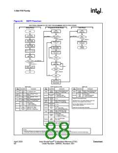
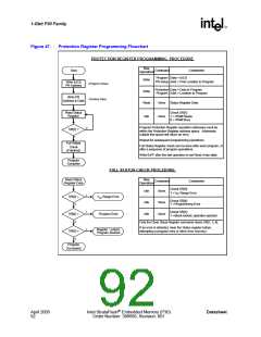
Figure 47.
Protection Register Programming Flowchart
PROTECTION REGISTER PROGRAMMING PROCEDURE
Bus
Operation
Start
Command
Comments
Program Data = 0xC0
PR Setup Addr = First Location to Program
Write
Write 0xC0,
PR Address
(Program Setup)
(Confirm Data)
Protection Data = Data to Program
Program Addr = Location to Program
Write
Read
Write PR
Address & Data
None
None
Status Register Data.
Read Status
Register
Check SR[7]:
1 = WSM Ready
0 = WSM Busy
Idle
Program Protection Register operation addresses must be
within the Protection Register address space. Addresses
outside this space will return an error.
0
SR[7] =
1
Repeat for subsequent programming operations.
Full Status
Check
(if desired)
Full Status Register check can be done after each program, or
after a sequence of program operations.
Write 0xFF after the last operation to set Read Array state.
Program
Complete
FULL STATUS CHECK PROCEDURE
Read Status
Register Data
Bus
Operation
Command
Comments
Check SR[3]:
1 =VPP Range Error
Idle
Idle
Idle
None
1
1
1
SR[3] =
0
VPP Range Error
Check SR[4]:
1 =Programming Error
None
None
Check SR[1]:
1 =Block locked; operation aborted
SR[4] =
0
Program Error
Only the Clear Staus Register command clears SR[1, 3, 4].
If an error is detected, clear the Status register before
attempting a program retry or other error recovery.
Register Locked;
Program Aborted
SR[1] =
0
Program
Successful
April 2005
92
Intel StrataFlash® Embedded Memory (P30)
Order Number: 306666, Revision: 001
Datasheet

 INTEL [ INTEL ]