1-Gbit P30 Family
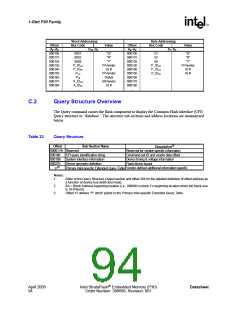
Word Addressing:
Hex Code
D15–D0
0051
0052
0059
P_IDLO
P_IDHI
PLO
Byte Addressing:
Offset
AX–A0
Value
Offset
AX–A0
Hex Code
D7–D0
51
52
59
P_IDLO
P_IDLO
P_IDHI
...
Value
00010h
00011h
00012h
00013h
00014h
00015h
00016h
00017h
00018h
...
"Q"
"R"
"Y"
00010h
00011h
00012h
00013h
00014h
00015h
00016h
00017h
00018h
...
"Q"
"R"
"Y"
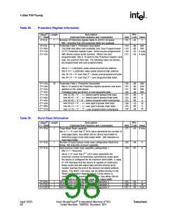
PrVendor
ID #
PrVendor
TblAdr
AltVendor
ID #
PrVendor
ID #
ID #
PHI
...
A_IDLO
A_IDHI
...
...
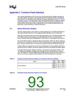
C.2
Query Structure Overview
The Query command causes the flash component to display the Common Flash Interface (CFI)
Query structure or “database.” The structure sub-sections and address locations are summarized
below.
Table 33.
Query Structure
Description(1)
Reserved for vendor-specific information
Command set ID and vendor data offset
Device timing & voltage information
Flash device layout
Offset
00001-Fh Reserved
00010h
0001Bh System interface information
00027h
P(3)
Sub-Section Name
CFI query identification string
Device geometry definition
Primary Intel-specific Extended Query Table
Vendor-defined additional information specific
Notes:
1.
2.
3.
Refer to the Query Structure Output section and offset 28h for the detailed definition of offset address as
a function of device bus width and mode.
BA = Block Address beginning location (i.e., 08000h is block 1’s beginning location when the block size
is 16-KWord).
Offset 15 defines “P” which points to the Primary Intel-specific Extended Query Table.
April 2005
94
Intel StrataFlash® Embedded Memory (P30)
Order Number: 306666, Revision: 001
Datasheet

 INTEL [ INTEL ]