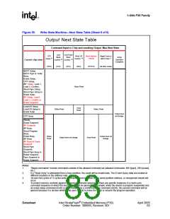
1-Gbit P30 Family
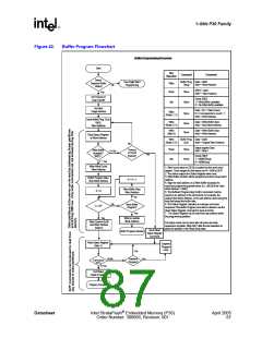
Figure 42.
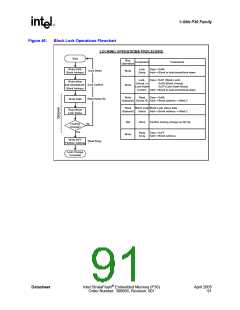
Buffer Program Flowchart
Buffer Programming Procedure
Start
Bus
Operation
Command
Comments
Device
Supports Buffer
Writes?
Use Single Word
Programming
Buffer Prog. Data = 0xE8
Write
Setup
Addr = Word Address
No
SR[7] = Valid
Addr = Word Address
Read
Idle
None
Yes
Set Timeout or
Loop Counter
Check SR[7]:
1 = Write Buffer available
0 = No Write Buffer available
None
None
Get Next
Target Address
Data = N-1 = Word Count
N = 0 corresponds to count = 1
Addr = Word Address
Write
(Notes 1, 2)
Issue Buffer Prog. Cmd.
0xE8,
Write
(Notes 3, 4)
Data = Write Buffer Data
Addr = Start Word Address
None
None
Word Address
Write
(Note 3)
Data = Write Buffer Data
Addr = Word Address
Read Status Register
at Word Address
Write
Buffer Prog. Data = 0xD0
(Notes 5, 6)
Conf.
Addr = Original Word Address
No
Status register Data
Addr = Note 7
Read
Idle
None
Timeout
or Count
Expired?
Write Buffer
0 = No
Available?
SR[7] =
Yes
Check SR[7]:
1 = WSM Ready
0 = WSM Busy
None
1 = Yes
Write Word Count,
Word Address
1. Word count value on D[7:0] is loaded into the word count
register. Count ranges for this device are N = 0x00 to 0x1F.
2. The device outputs the Status Register when read.
3. Write Buffer contents will be programmed at the issued word
address.
4. Align the start address on a Write Buffer boundary for
maximum programming performance (i.e., A[4:0] of the Start
Word Address = 0x00).
5. The Buffered Programming Confirm command must be
issued to an address in the same block, for example, the
original Start Word Address, or the last address used during the
loop that loaded the buffer data.
Buffer Program Data,
Start Word Address
X = X + 1
Write Buffer Data,
Word Address
X = 0
No
No
6. The Status Register indicates an improper command
sequence if the Buffer Program command is aborted; use the
Clear Status Register command to clear error bits.
7. The Status Register can be read from any address within
the programming partition.
Abort Buffer
Program?
X = N?
Yes
Yes
Write to another
Block Address
Write Confirm 0xD0
and Word Address
(Note 5)
Full status check can be done after all erase and write
sequences complete. Write 0xFF after the last operation to
place the partition in the Read Array state.
Issue Read
Status Register
Command
Buffer Program Aborted
Read Status Register
(Note 7)
Suspend
Program
Loop
No
0=No
Yes
Suspend
Program?
Is BP finished?
SR[7] =
1=Yes
Full Status
Check if Desired
Program Complete
Datasheet
Intel StrataFlash® Embedded Memory (P30)
Order Number: 306666, Revision: 001
April 2005
87

 INTEL [ INTEL ]