28F010
ABSOLUTE MAXIMUM RATINGS*
NOTICE: This is a production data sheet. The specifi-
cations are subject to change without notice.
Operating Temperature
During Read ÀÀÀÀÀÀÀÀÀÀÀÀÀÀÀÀÀÀ0 C to 70 C
*WARNING: Stressing the device beyond the ‘‘Absolute
Maximum Ratings’’ may cause permanent damage.
These are stress ratings only. Operation beyond the
‘‘Operating Conditions’’ is not recommended and ex-
tended exposure beyond the ‘‘Operating Conditions’’
may affect device reliability.
(1)
(1)
a
§
§
a
During Erase/Program ÀÀÀÀÀÀÀÀÀ0 C to 70 C
§
§
Operating Temperature
During Read ÀÀÀÀÀÀÀÀÀÀÀÀÀÀÀ 40 C to 85 C
(2)
(2)
(1)
(2)
b
a
§
§
b
a
During Erase/Program ÀÀÀÀÀÀ 40 C to 85 C
§
§
b
a
Temperature Under BiasÀÀÀÀÀÀÀ 10 C to 80 C
§
§
b
a
a
Temperature Under BiasÀÀÀÀÀÀÀ 50 C to 95 C
§
§
b
Storage Temperature ÀÀÀÀÀÀÀÀÀÀ 65 C to 125 C
§
§
Voltage on Any Pin with
Respect to Ground ÀÀÀÀÀÀÀÀÀÀ 2.0V to 7.0V
Voltage on Pin A with
(3)
b
a
9
(3, 4)
b
a
Respect to Ground ÀÀÀÀÀÀÀ 2.0V to 13.5V
Supply Voltage with
V
PP
Respect to Ground
During Erase/ProgramÀÀÀÀ 2.0V to 14.0V
Supply Voltage with
(3, 4)
b
a
V
CC
(3)
b
a
Respect to Ground ÀÀÀÀÀÀÀÀÀÀ 2.0V to 7.0V
Output Short Circuit CurrentÀÀÀÀÀÀÀÀÀÀÀÀÀ100 mA
(5)
OPERATING CONDITIONS
Limits
Unit
Max
Symbol
Parameter
Min
(1)
T
A
Operating Temperature
0
70
C
C
§
§
(2)
b
a
85
T
A
Operating Temperature
40
(6)
V
V
V
Supply Voltage (10%)
4.50
4.75
5.50
5.25
V
CC
CC
CC
(7)
V
Supply Voltage (5%)
V
CC
NOTES:
1. Operating Temperature is for commercial product as defined by this specification.
2. Operating Temperature is for extended temperature products as defined by this specification.
b
b
3. Minimum DC input voltage is 0.5V. During transitions, inputs may undershoot to 2.0V for periods less
than 20 ns. Maximum DC voltage on output pins is V
a
a
0.5V, which may overshoot to V
2.0V for
CC
CC
periods less than 20 ns.
4. Maximum DC voltage on A or V may overshoot to 14.0V for periods less than 20 ns.
a
5. Output shorted for no more than one second. No more than one output shorted at a time.
9
PP
6. See High Speed AC Input/Output reference Waveforms and High Speed AC Testing Load Circuits for
testing characteristics.
7. See AC Input/Output reference Waveforms and AC Testing Load Circuits for testing characteristics.
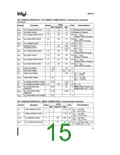
DC CHARACTERISTICSÐTTL/NMOS COMPATIBLEÐCommercial Products
Limits
Symbol
Parameter
Notes
Unit
Test Conditions
(4)
Min Typical
Max
e
V
g
I
I
I
I
Input Leakage Current
Output Leakage Current
1
1
1
1
1.0
mA
V
V
V
Max
CC
or V
LI
CC
IN
e
CC
SS
e
g
10
1.0
30
mA
V
V
V
V
Max
CC
LO
CC
e
or V
OUT
CC
SS
e
V
V
Standby Current
0.3
10
mA
mA
V
CC
CE
V
V
IH
Max
CC
CCS
CC1
CC
CC
e
Ý
e
6 MHz, I
e
Ý
V
0 mA
Active Read Current
V
V
Max, CE
e
CC
CC
IL
e
f
OUT
14

 INTEL [ INTEL ]