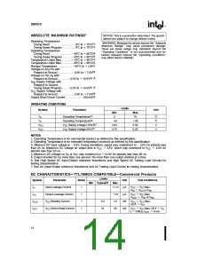
28F010
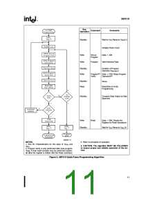
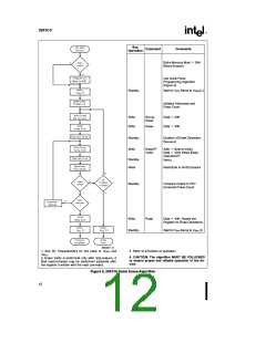
Bus
Operation
Command
Comments
e
Entire Memory Must
Before Erasure
00H
Use Quick Pulse
Programming Algorithm
(Figure 5)
Standby
Wait for V Ramp to V (1)
PP PPH
Initialize Addresses and
Pulse-Count
e
e
Write
Write
Set-up
Erase
Data
Data
20H
20H
Erase
Standby
Write
Duration of Erase Operation
)
(t
WHWH2
(2)
e
e
Erase
Verify
Addr
Data
Byte to Verify;
A0H; Stops Erase
(3)
Operation
t
WHGL
Standby
Read
Read Byte to Verify Erasure
Standby
Compare Output to FFH
Increment Pulse-Count
e
Data 00H, Resets the
Register for Read Operations
Write
Read
Standby
Wait for V Ramp to V (1)
PP PPL
290207–6
1. See DC Characteristics for the value of V and
3. Refer to principles of operation.
PPH
V
.
PPL
4. CAUTION: The algorithm MUST BE FOLLOWED
to ensure proper and reliable operation of the de-
vice.
2. Erase Verify is performed only after chip-erasure. A
final read/compare may be performed (optional) after
the register is written with the read command.
Figure 6. 28F010 Quick Erase Algorithm
12

 INTEL [ INTEL ]