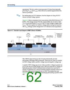
Power-On Reset Circuitry
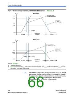
Figure 4–5. Power-Up Characteristics for MAX II & MAX II G Devices
Notes (1), (2)
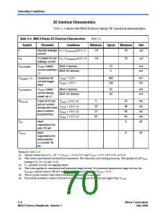
MAX II Device
V
CCINT
Approximate Voltage
for SRAM Download Start
3.3 V
2.5 V
Device Resets
the SRAM and
Tri-States I/O Pins
1.7 V
1.4 V
t
CONFIG
0 V
User Mode
Operation
Tri-State
Tri-State
MAX II G Device
V
CCINT
3.3 V
1.8 V
Approximate Voltage
for SRAM Download Start
Device Resets
the SRAM and
Tri-States I/O Pins
1.55 V
1.4 V
t
CONFIG
0 V
User Mode
Operation
Tri-State
Tri-State
Notes to Figure 4–5:
(1) Time scale is relative.
(2) Figure 4–5 assumes all VCCIO banks power simultaneously with the VCCINT profile shown. If not, tCONFIG stretches
out until all VCCIO banks are powered.
1
After SRAM configuration, all registers in the device are cleared
and released into user function before I/O tri-states are released.
To release clears after tri-states are released, use the DEV_CLRn
pin option. To hold the tri-states beyond the power-up
configuration time, use the DEV_OEpin option.
4–8
MAX II Device Handbook, Volume 1
Core Version a.b.c variable
Altera Corporation
February 2006

 INTEL [ INTEL ]