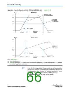
Operating Conditions
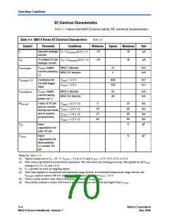
DC Electrical Characteristics
Table 5–4 shows the MAX II device family DC electrical characteristics.
Table 5–4. MAX II Device DC Electrical Characteristics
Note (1)
Symbol
Parameter
Conditions
Minimum
Typical
Maximum
Unit
II
Input pin leakage
current
–10
10
μA
VI = VCCIOmax to 0 V (2)
IOZ
Tri-stated I/O pin
leakage current
–10
10
μA
VO = VCCIOmax to 0 V (2)
ICCSTANDBY
VCCINT supply
current (standby)
(3)
MAX II devices
12
2
mA
mA
MAX IIG devices
Hysteresis for
Schmitt trigger
input
V
CCIO = 3.3 V
CCIO = 2.5 V
400
190
mV
mV
VSCHMITT (4)
V
ICCPOWERUP
VCCINT supply
current during
power-up (5)
MAX II devices
55
40
mA
mA
MAX IIG devices
RPULLUP
Value of I/O pin
pull-up resistor
duringusermode
and in-system
programming
5
25
40
60
95
8
kΩ
kΩ
kΩ
kΩ
pF
V
CCIO = 3.3 V (6)
10
25
45
VCCIO = 2.5 V (6)
VCCIO = 1.8 V (6)
VCCIO = 1.5 V (6)
CIO
Input
capacitance for
user I/O pin
CGCLK
Input
8
pF
capacitance for
dual-purpose
GCLK/user I/O
pin
Notes to Table 5–4:
(1) Typical values are for TA = 25 ° C, VCCINT = 3.3 or 2.5 V, and VCCIO = 1.5 V, 1.8 V, 2.5 V, or 3.3 V.
(2) This value is specified for normal device operation. The value may vary during power-up. This applies for all VCCIO
settings (3.3, 2.5, 1.8, and 1.5 V).
(3) VI = ground, no load, no toggling inputs.
(4) This value applies to commercial and industrial range devices. For extended temperature range devices, the
VSCHMITT typical value is 300 mV for VCCIO = 3.3 V and 120 mV for VCCIO = 2.5 V.
(5) This is a peak current value with a maximum duration of tCONFIG time.
(6) Pin pull-up resistance values will lower if an external source drives the pin higher than VCCIO
.
5–4
Core Version a.b.c variable
Altera Corporation
July 2006
MAX II Device Handbook, Volume 1

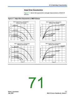
 INTEL [ INTEL ]