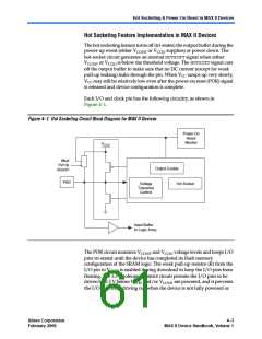
Hot Socketing & Power-On Reset in MAX II Devices
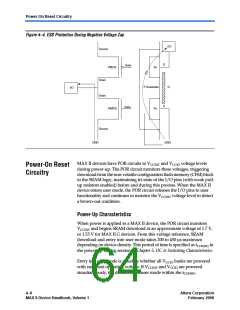
specifications. If VCCIO is powered more than tCONFIG after VCCINT, the
device does not enter user mode until 2 µs after all VCCIO banks are
powered.
In user mode, the POR circuitry continues to monitor the VCCINT (but not
VCCIO) voltage level to detect a brown-out condition. If there is a VCCINT
voltage sag at or below 1.4 V during user mode, the POR circuit resets the
SRAM and tri-states the I/O pins. Once VCCINT rises back to
approximately 1.7 V (or 1.55 V for MAX II G devices), the SRAM
download restarts and the device begins to operate after tCONFIG time has
passed.
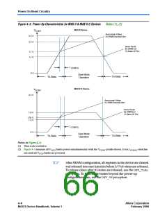
Figure 4–5 shows the voltages for MAX II and MAX II G device POR
during power-up into user mode and from user mode to power-down or
brown-out.
Altera Corporation
February 2006
Core Version a.b.c variable
4–7
MAX II Device Handbook, Volume 1

 INTEL [ INTEL ]