Hot Socketing & Power-On Reset in MAX II Devices
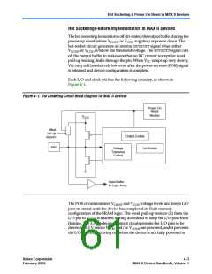
Hot Socketing Feature Implementation in MAX II Devices
The hot socketing feature turns off (tri-states) the output buffer during the
power-up event (either VCCINT or VCCIO supplies) or power down. The
hot-socket circuit generates an internal HOTSCKTsignal when either
VCCINT or VCCIO is below the threshold voltage. The HOTSCKTsignal cuts
off the output buffer to make sure that no DC current (except for weak
pull-up leaking) leaks through the pin. When VCC ramps up very slowly,
VCC may still be relatively low even after the power-on reset (POR) signal
is released and device configuration is complete.
Each I/O and clock pin has the following circuitry, as shown in
Figure 4–1.
Figure 4–1. Hot Socketing Circuit Block Diagram for MAX II Devices
Power On
Reset
Monitor
VCCIO
Weak
Pull-Up
Resistor
Output Enable
PAD
Voltage
Tolerance
Control
Hot Socket
Input Buffer
to Logic Array
The POR circuit monitors VCCINT and VCCIO voltage levels and keeps I/O
pins tri-stated until the device has completed its flash memory
configuration of the SRAM logic. The weak pull-up resistor (R) from the
I/O pin to VCCIO is enabled during download to keep the I/O pins from
floating. The 3.3-V tolerance control circuit permits the I/O pins to be
driven by 3.3 V before VCCIO and/or VCCINT are powered, and it prevents
the I/O pins from driving out when the device is not fully powered or
Altera Corporation
February 2006
Core Version a.b.c variable
4–3
MAX II Device Handbook, Volume 1

 INTEL [ INTEL ]